ZHCSKE6C July 2019 – February 2020 TPS63810 , TPS63811
PRODUCTION DATA.
- 1 特性
- 2 应用
- 3 说明
- 4 修订历史记录
- 5 器件比较表
- 6 Pin Configuration and Functions
- 7 Specifications
-
8 Detailed Description
- 8.1 Overview
- 8.2 Functional Block Diagram
- 8.3
Feature Description
- 8.3.1 Control Scheme
- 8.3.2 Control Scheme
- 8.3.3 Power-Save Mode Operation (PSM)
- 8.3.4 Forced-PWM Operation (FPWM)
- 8.3.5 Ramp-PWM Operation (RPWM)
- 8.3.6 Device Enable (EN)
- 8.3.7 Undervoltage Lockout (UVLO)
- 8.3.8 Soft Start
- 8.3.9 Output Voltage Control
- 8.3.10 Protection Functions
- 8.3.11 Power Good
- 8.3.12 Load Disconnect
- 8.3.13 Output Discharge
- 8.4 Device Functional Modes
- 8.5 Programming
- 8.6
Register Map
- 8.6.1
Register Description
- 8.6.1.1 Register Map
- 8.6.1.2 Register CONTROL (Slave address: 0b1110101; Register address: 0x01; Default: 0x00 or 0x20)
- 8.6.1.3 Register STATUS (Slave address: 0b1110101; Register address: 0x02; Default: 0x00)
- 8.6.1.4 Register DEVID (Slave address: 0b1110101; Register address: 0x03; Default: 0x04)
- 8.6.1.5 Register VOUT1 (Slave address: 0b1110101; Register address: 0x04; Default: 0x3C)
- 8.6.1.6 Register VOUT2 (Slave address: 0b1110101; Register address: 0x05; Default: 0x42)
- 8.6.1
Register Description
- 9 Application and Implementation
- 10Power Supply Recommendations
- 11Layout
- 12器件和文档支持
- 13机械、封装和可订购信息
8.5.2 Standard-, Fast-, and Fast-Mode Plus Protocol
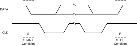
The master initiates a data transfer by generating a start condition. The start condition is when a high-to-low transition occurs on the SDA line while SCL is high, as shown in Figure 20. All I2C-compatible devices recognize a start condition.
 Figure 20. START and STOP Conditions
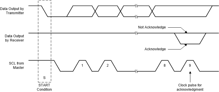
 The master then generates the SCL pulses and transmits the 7-bit address and the read/write direction bit, R/W, on the SDA line. During all transmissions, the master ensures that data is valid. A valid data condition requires the SDA line to be stable during the entire high period of the clock pulse (see Figure 21). All devices recognize the address sent by the master and compare it to their internal fixed addresses. Only the slave device with a matching address generates an acknowledge (see Figure 22) by pulling the SDA line low during the entire high period of the ninth SCL cycle. Upon detecting this acknowledge, the master knows that communication link with a slave has been established.
 Figure 21. Bit Transfer on the Serial Interface
 The master generates further SCL cycles to either transmit data to the slave (R/W bit 1) or receive data from the slave (R/W bit 0). In either case, the receiver needs to acknowledge the data sent by the transmitter. An acknowledge signal can either be generated by the master or by the slave, depending on which one is the receiver. 9-bit valid data sequences consisting of 8-bit data and 1-bit acknowledge can continue as long as necessary.
To signal the end of the data transfer, the master generates a stop condition by pulling the SDA line from low to high while the SCL line is high (see Figure 20). This releases the bus and stops the communication link with the addressed slave. All I2C-compatible devices must recognize the stop condition. Upon the receipt of a stop condition, all devices know that the bus is released and they wait for a start condition followed by a matching address.
Attempting to read data from register addresses not listed in this section results in 00h being read out.
 Figure 22. Acknowledge on the I2C Bus
  Figure 23. Bus Protocol