ZHCSCN2 July 2014 TPS57114-EP
PRODUCTION DATA.
- 1 特性
- 2 应用范围
- 3 说明
- 4 简化电路原理图
- 5 修订历史记录
- 6 说明(续)
- 7 Pin Configuration and Functions
- 8 Specifications
-
9 Detailed Description
- 9.1 Overview
- 9.2 Functional Block Diagram
- 9.3
Feature Description
- 9.3.1 Fixed-Frequency Pwm Control
- 9.3.2 Slope Compensation and Output Current
- 9.3.3 Bootstrap Voltage (Boot) and Low-Dropout Operation
- 9.3.4 Error Amplifier
- 9.3.5 Voltage Reference
- 9.3.6 Adjusting the Output Voltage
- 9.3.7 Enable Functionality and Adjusting UVLO
- 9.3.8 Slow-Start or Tracking Pin
- 9.3.9 Constant Switching Frequency and Timing Resistor (RT/CLK Pin)
- 9.3.10 Overcurrent Protection
- 9.3.11 Frequency Shift
- 9.3.12 Reverse Overcurrent Protection
- 9.3.13 Synchronize Using the RT/CLK Pin
- 9.3.14 Power Good (PWRGD Pin)
- 9.3.15 Overvoltage Transient Protection (OVTP)
- 9.3.16 Thermal Shutdown
- 9.3.17 Small-Signal Model for Loop Response
- 9.3.18 Simple Small-Signal Model for Peak-Current Mode Control
- 9.3.19 Small-Signal Model for Frequency Compensation
- 9.4 Device Functional Modes
-
10Application and Implementation
- 10.1 Application Information
- 10.2
Typical Application
- 10.2.1 Design Requirements
- 10.2.2
Detailed Design Procedure
- 10.2.2.1 Selecting the Switching Frequency
- 10.2.2.2 Output Inductor Selection
- 10.2.2.3 Output Capacitor
- 10.2.2.4 Input Capacitor
- 10.2.2.5 Slow-Start Capacitor
- 10.2.2.6 Bootstrap Capacitor Selection
- 10.2.2.7 Output-Voltage and Feedback-Resistor Selection
- 10.2.2.8 Compensation
- 10.2.2.9 Power-Dissipation Estimate
- 10.2.3 Application Curves
- 11Power Supply Recommendations
- 12Layout
- 13器件和文档支持
- 14机械封装和可订购信息
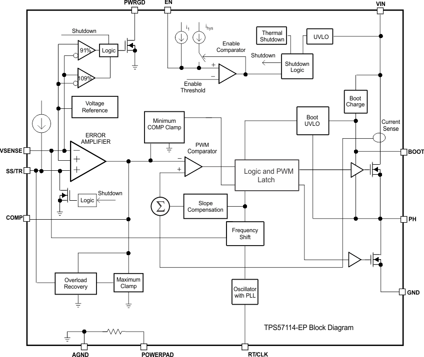
9 Detailed Description
9.1 Overview
The TPS57114-EP is a 6-V, 3.5-A, synchronous step-down (buck) converter with two integrated N-channel MOSFETs. To improve performance during line and load transients, the device implements a constant-frequency, peak-current mode control which reduces output capacitance and simplifies external frequency-compensation design. The wide switching-frequency range of 200 to 2000 kHz allows for efficiency and size optimization when selecting the output-filter components. Adjust the switching frequency using a resistor to ground on the RT/CLK pin. The device has an internal phase-lock loop (PLL) on the RT/CLK pin that synchronizes the power-switch turn-on to the falling edge of an external system clock.
The TPS57114-EP has a typical default start-up voltage of 2.45 V. The EN pin has an internal pullup current source; to adjust the input-voltage UVLO, use two external resistors on the EN pin. In addition, the pullup current provides a default condition, allowing the device to operate when the EN pin is floating. The total operating current for the TPS57114-EP is typically 515 µA when not switching and under no load. When the device is disabled, the supply current is less than 5.5 µA.
The integrated 12-mΩ MOSFETs allow for high-efficiency power-supply designs with continuous output currents up to 3.5 A.
The TPS57114-EP reduces the external component count by integrating the boot recharge diode. A capacitor between the BOOT and PH pins supplies the bias voltage for the integrated high-side MOSFET. A UVLO circuit, which monitors the boot-capacitor voltage, turns off the high-side MOSFET when the voltage falls below a preset threshold. This BOOT circuit allows the TPS57114-EP to operate approaching 100% duty cycle. The output voltage can be stepped down to as low as the 0.8-V reference.
The TPS57114-EP has a power-good comparator (PWRGD) with 2% hysteresis.
The TPS57114-EP minimizes excessive output overvoltage transients by taking advantage of the overvoltage power-good comparator. The regulated output voltage exceeding 109% of the nominal voltage activates the overvoltage comparator, which turns off the high-side MOSFET and masks it from turning on until the output voltage is lower than 107% of the nominal voltage.
The SS/TR (slow-start or tracking) pin minimizes inrush currents or provides power-supply sequencing during power-up. Connect a small-value capacitor to the pin for slow start. Discharging the SS/TR pin before the output powers up ensures a repeatable restart after an overtemperature fault, UVLO fault, or disabled condition.
The use of a frequency-foldback circuit reduces the switching frequency during start-up and overcurrent fault conditions to help limit the inductor current.
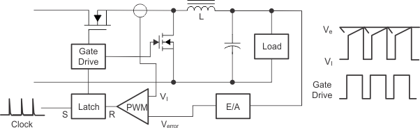 Figure 22. Peak Current Mode Control (See Application Note U-140)
9.2 Functional Block Diagram
9.3 Feature Description
9.3.1 Fixed-Frequency Pwm Control
The TPS57114-EP uses an adjustable fixed-frequency peak-current mode control. An error amplifier, which drives the COMP pin, compares the output voltage through external resistors on the VSENSE pin to an internal voltage reference. An internal oscillator initiates the turn-on of the high-side power switch. The device compares the error-amplifier output to the high-side power-switch current. When the power-switch current reaches the COMP voltage level, the high-side power switch turns off and the low-side power switch turns on. The COMP pin voltage increases and decreases as the output current increases and decreases. The device implements a current limit by clamping the COMP pin voltage to a maximum level, and also implements a minimum clamp for improved transient-response performance.
9.3.2 Slope Compensation and Output Current
The TPS57114-EP adds a compensating ramp to the switch-current signal. This slope compensation prevents subharmonic oscillations as the duty cycle increases. The available peak inductor current remains constant over the full duty-cycle range.
9.3.3 Bootstrap Voltage (Boot) and Low-Dropout Operation
The TPS57114-EP has an integrated boot regulator and requires a small ceramic capacitor between the BOOT and PH pins to provide the gate-drive voltage for the high-side MOSFET. The value of the ceramic capacitor should be 0.1 µF. TI recommends a ceramic capacitor with an X7R or X5R grade dielectric and a voltage rating of 10 V or higher because of the stable characteristics over temperature and voltage.
To improve dropout, the design of the TPS57114-EP is for operation at 100% duty cycle as long as the BOOT-to-PH pin voltage is greater than 2.2 V. A UVLO circuit turns off the high-side MOSFET, allowing for the low-side MOSFET to conduct when the voltage from BOOT to PH drops below 2.2 V. Because the supply current sourced from the BOOT pin is low, the high-side MOSFET can remain on for more switching cycles than are required to refresh the capacitor; thus, the effective duty cycle of the switching regulator is high.
9.3.4 Error Amplifier
The TPS57114-EP has a transconductance amplifier which it uses as an error amplifier. The error amplifier compares the VSENSE voltage to the lower of the SS/TR pin voltage or the internal 0.8-V voltage reference. The transconductance of the error amplifier is 245 µS during normal operation. When the voltage of the VSENSE pin is below 0.8 V and the device is regulating using the SS/TR voltage, the gm is typically greater than 79 µS, but less than 245 µS.
9.3.5 Voltage Reference
The voltage-reference system produces a precise ±1% voltage reference over temperature by scaling the output of a temperature-stable band-gap circuit. The band-gap and scaling circuits produce 0.8 V at the non-inverting input of the error amplifier.
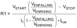
9.3.6 Adjusting the Output Voltage
A resistor divider from the output node to the VSENSE pin sets the output voltage. TI recommends using divider resistors with 1% tolerance or better. Start with 100 kΩ for the R1 resistor and use Equation 1 to calculate R2. To improve efficiency at light loads, consider using larger-value resistors. If the values are too high, the regulator is more susceptible to noise, and voltage errors from the VSENSE input current are noticeable.
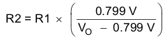
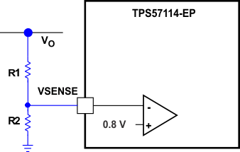 Figure 23. Voltage-Divider Circuit
9.3.7 Enable Functionality and Adjusting UVLO
The VIN pin voltage falling below 2.6 V disables the TPS57114-EP. If an application requires a higher UVLO, use the EN pin as shown in Figure 24 to adjust the input voltage UVLO by connecting two external resistors. TI recommends using the EN resistors to set the UVLO falling threshold (VSTOP) above 2.6 V. Set the rising threshold (VSTART) to provide enough hysteresis to allow for any input supply variations. The EN pin has an internal pullup current source that provides the default condition of the TPS57114-EP operating when the EN pin floats. When the EN pin voltage exceeds 1.25 V, the circuitry adds an additional 1.6 µA of hysteresis. Pulling the EN pin below 1.18 V removes the 1.6 µA. This additional current facilitates input voltage hysteresis.
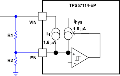 Figure 24. Adjustable UVLO
where
- Ihys = 1.6 µA
- I1 = 1.6 µA
- VENRISING = 1.25 V
- VENFALLING = 1.18 V
9.3.8 Slow-Start or Tracking Pin
The TPS57114-EP regulates to the lower of the SS/TR pin and the internal reference voltage. A capacitor on the SS/TR pin to ground implements a slow-start time. The TPS57114-EP has an internal pullup current source of 2 µA which charges the external slow-start capacitor. Equation 4 calculates the required slow-start capacitor value.

where
- Tss is the desired slow-start time in ms
- Iss is the internal slow-start charging current of 2 µA
- Vref is the internal voltage reference of 0.8 V
If during normal operation VIN goes below UVLO, the EN pin goes below 1.2 V, or a thermal shutdown event occurs, the TPS57114-EP stops switching. Upon VIN going above UVLO, the release or pulling high of EN, or the exit of a thermal shutdown, SS/TR discharges to below 60 mV before reinitiating a powering-up sequence. The VSENSE voltage follows the SS/TR pin voltage with a 54-mV offset up to 85% of the internal voltage reference. When the SS/TR voltage is greater than 85% on the internal reference voltage, the offset increases as the effective system reference transitions from the SS/TR voltage to the internal voltage reference.
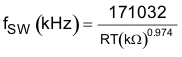
9.3.9 Constant Switching Frequency and Timing Resistor (RT/CLK Pin)
The switching frequency of the TPS57114-EP is adjustable over a wide range from 300 to 2000 kHz by placing a maximum of 700 kΩ or minimum of 85 kΩ, respectively, on the RT/CLK pin. An internal amplifier holds this pin at a fixed voltage when using an external resistor to ground to set the switching frequency. The RT/CLK is typically 0.5 V. To determine the timing resistance for a given switching frequency, use the curve in Figure 6 or Equation 5.
To reduce the solution size, one would typically set the switching frequency as high as possible, but consider tradeoffs of the efficiency, maximum input voltage, and minimum controllable on-time.
The minimum controllable on-time is typically 65 ns at full-current load and 120 ns at no load and limits the maximum operating input voltage or output voltage.
9.3.10 Overcurrent Protection
The TPS57114-EP implements a cycle-by-cycle current limit. During each switching cycle, the device compares the high-side switch current to the voltage on the COMP pin. When the instantaneous switch current intersects the COMP voltage, the high-side switch turns off. During overcurrent conditions that pull the output voltage low, the error amplifier responds by driving the COMP pin high, increasing the switch current. There is an internal clamp on the error-amplifier output. This clamp functions as a switch-current limit.
9.3.11 Frequency Shift
To operate at high switching frequencies and provide protection during overcurrent conditions, the TPS57114-EP implements a frequency shift. Without this frequency shift, during an overcurrent condition the low-side MOSFET may not turn off long enough to reduce the current in the inductor, causing a current runaway. With frequency shift, during an overcurrent condition there is a switching frequency reduction from 100% to 50%, then 25%, as the voltage decreases from 0.8 to 0 V on the VSENSE pin, to allow the low-side MOSFET to be off long enough to decrease the current in the inductor. During start-up, the switching frequency increases as the voltage on VSENSE increases from 0 to 0.8 V. See Figure 7 for details.
9.3.12 Reverse Overcurrent Protection
The TPS57114-EP implements low-side current protection by detecting the voltage across the low-side MOSFET. When the converter sinks current through its low-side FET, the control circuit turns off the low-side MOSFET if the reverse current is typically more than 4.5 A. By implementing this additional protection scheme, the converter is able to protect itself from excessive current during power cycling and start-up into prebiased outputs.
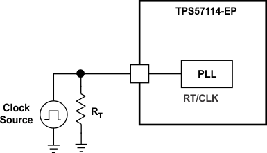
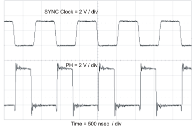
9.3.13 Synchronize Using the RT/CLK Pin
The RT/CLK pin synchronizes the converter to an external system clock (see Figure 25). To implement the synchronization feature in a system, connect a square wave to the RT/CLK pin with an on-time of at least 75 ns. If the pin goes above the PLL upper threshold, a mode change occurs, and the pin becomes a synchronization input. The device disables the internal amplifier, and the pin is a high-impedance clock input to the internal PLL. If clocking edges stop, the device re-enables the internal amplifier and the mode returns to the frequency set by the resistor. The square-wave amplitude at this pin must transition lower than 0.6 V and higher than 1.6 V, typically. The synchronization frequency range is 300 to 2000 kHz. The rising edge of PH synchronizes to the falling edge of the RT/CLK pin.
9.3.14 Power Good (PWRGD Pin)
The PWRGD pin output is an open-drain MOSFET. The output goes low when the VSENSE voltage enters the fault condition by falling below 91% or rising above 109% of the nominal internal reference voltage. There is a 2% hysteresis on the threshold voltage, so when the VSENSE voltage rises to the good condition above 93% or falls below 107% of the internal voltage reference, the PWRGD output MOSFET turns off. TI recommends to use a pullup resistor between 1 to 100 kΩ with a voltage source that is 6 V or less. PWRGD is in a valid state after the VIN input voltage is greater than 1.1 V.
9.3.15 Overvoltage Transient Protection (OVTP)
The TPS57114-EP incorporates an OVTP circuit to minimize voltage overshoot when recovering from output fault conditions or strong unload transients. The OVTP feature minimizes the output overshoot by implementing a circuit to compare the VSENSE pin voltage to the OVTP threshold, which is 109% of the internal voltage reference. The VSENSE pin voltage going greater than the OVTP threshold disables the high-side MOSFET, preventing current from flowing to the output and minimizing output overshoot. The VSENSE voltage dropping lower than the OVTP threshold allows the high-side MOSFET to turn on during the next clock cycle.
9.3.16 Thermal Shutdown
The device implements an internal thermal shutdown to protect itself if the junction temperature exceeds 168°C. The thermal shutdown forces the device to stop switching when the junction temperature exceeds the thermal trip threshold. When the die temperature decreases below 148°C, the device reinitiates the power-up sequence by discharging the SS pin to below 60 mV. The thermal shutdown hysteresis is 20°C.
9.3.17 Small-Signal Model for Loop Response
Figure 27 shows an equivalent model for the TPS57114-EP control loop which the user can model in a circuit-simulation program to check frequency response and dynamic load response. The error amplifier is a transconductance amplifier with a gm of 245 µS. The user can use an ideal voltage-controlled current source to model the error amplifier. Resistor R0 and capacitor C0 model the open-loop gain and frequency response of the amplifier. The 1-mV AC voltage source between nodes a and b effectively breaks the control loop for the frequency-response measurements. Plotting a or c versus frequency shows the small-signal response of the frequency compensation. Plotting a or b versus frequency shows the small-signal response of the overall loop. The user can check the dynamic loop response by replacing RL with a current source having the appropriate load-step amplitude and step rate in a time domain analysis.
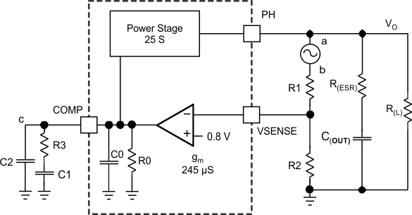 Figure 27. Small-Signal Model for Loop Response
9.3.18 Simple Small-Signal Model for Peak-Current Mode Control
Figure 27 is a simple small-signal model that the user can use to understand how to design the frequency compensation. An approximation of a voltage-controlled current source (duty-cycle modulator) supplying current to the output capacitor and load resistor can approximate the TPS57114-EP power stage. The control-to-output transfer function, shown in Equation 7, consists of a DC gain, one dominant pole, and one ESR zero. The quotient of the change in switch current divided by the change in COMP pin voltage (node c in Figure 27) is the power-stage transconductance. The gm for the TPS57114-EP is 25 S. The low-frequency gain of the power-stage frequency response is the product of the transconductance and the load resistance, as shown in Equation 8. As the load current increases and decreases, the low-frequency gain decreases and increases, respectively. This variation with load may seem problematic at first glance, but the dominant pole moves with load current (see Equation 9). The dashed line in the right half of Figure 28 highlights the combined effect. As the load current decreases, the gain increases and the pole frequency lowers, keeping the 0-dB crossover frequency the same for the varying load conditions, which makes it easier to design the frequency compensation.
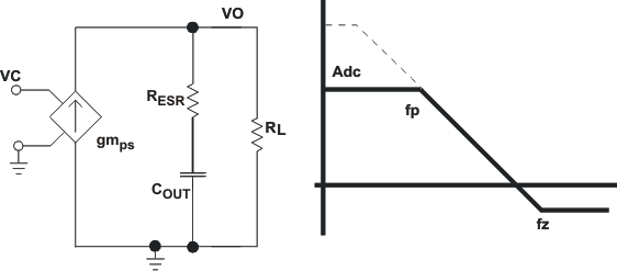 Figure 28. Simple Small-Signal Model and Frequency Response for Peak-Current Mode Control

9.3.19 Small-Signal Model for Frequency Compensation
The TPS57114-EP uses a transconductance amplifier for the error amplifier and readily supports two of the commonly used frequency-compensation circuits. Figure 29 shows the compensation circuits. High-bandwidth power-supply designs most likely implement Type 2 circuits using low-ESR output capacitors. In Type 2A, inclusion of one additional high-frequency pole attenuates high-frequency noise.
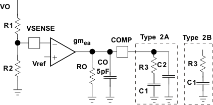 Figure 29. Types of Frequency Compensation
The design guidelines for TPS57114-EP loop compensation are as follows:
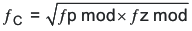
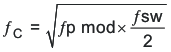
- Calculate the modulator pole, ƒpmod, and the ESR zero, ƒz1, using Equation 11 and Equation 12. If the output voltage is a high percentage of the capacitor rating, it may be necessary to derate the output capacitor (COUT). Use the manufacturer information for the capacitor to derate the capacitor value. Use Equation 13 and Equation 14 to estimate a starting point for the crossover frequency, ƒc. Equation 13 is the geometric mean of the modulator pole and the ESR zero and Equation 14 is the mean of the modulator pole and the switching frequency. Use the lower value of Equation 13 or Equation 14 as the maximum crossover frequency.
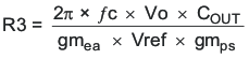
- Determine R3 with:
- gmea is the amplifier gain (245 µS)
- gmps is the power stage gain (25 S)
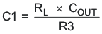
- Place a compensation zero at the dominant pole
 . Determine C1 with:
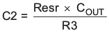
 - C2 is optional. Use it, if necessary, to cancel the 0 from the ESR of COUT.
where
9.4 Device Functional Modes
9.4.1 RT (Resistor Timing) Mode
External resistor to ground can be connected to the RT/CLK pin, which enables the user to adjust the switching frequency. The device has an internal PLL on the RT/CLK pin that synchronizes the power-switch turn on to the falling edge of an external system clock. The frequency is adjustable from 200 to 2000 kHz by using external resistor maximum of 700 kΩ or minimum of 85 kΩ (see Constant Switching Frequency and Timing Resistor (RT/CLK Pin)).
9.4.2 CLK (External Clock) Mode
The RT/CLK pin synchronizes the converter to an external system clock. To implement the synchronization feature in a system, connect a square wave to the RT/CLK pin with an on-time of at least 75 ns. If the pin goes above the PLL upper threshold, a mode change occurs, and the pin becomes a synchronization input. The device disables the internal amplifier and the terminal is a high-impedance clock input to the internal PLL. If clocking edges stop, the device re-enables the internal amplifier and the mode returns to the frequency set by the resistor. The square-wave amplitude at this pin must transition lower than 0.6 V and higher than 1.6 V, typically. The synchronization frequency range is 300 to 2000 kHz. The rising edge of PH synchronizes to the falling edge of the RT/CLK pin.