ZHCSCN2 July 2014 TPS57114-EP
PRODUCTION DATA.
- 1 特性
- 2 应用范围
- 3 说明
- 4 简化电路原理图
- 5 修订历史记录
- 6 说明(续)
- 7 Pin Configuration and Functions
- 8 Specifications
-
9 Detailed Description
- 9.1 Overview
- 9.2 Functional Block Diagram
- 9.3
Feature Description
- 9.3.1 Fixed-Frequency Pwm Control
- 9.3.2 Slope Compensation and Output Current
- 9.3.3 Bootstrap Voltage (Boot) and Low-Dropout Operation
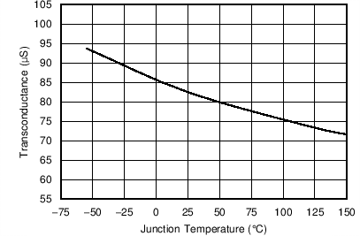
- 9.3.4 Error Amplifier
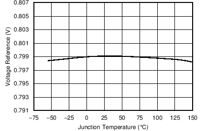
- 9.3.5 Voltage Reference
- 9.3.6 Adjusting the Output Voltage
- 9.3.7 Enable Functionality and Adjusting UVLO
- 9.3.8 Slow-Start or Tracking Pin
- 9.3.9 Constant Switching Frequency and Timing Resistor (RT/CLK Pin)
- 9.3.10 Overcurrent Protection
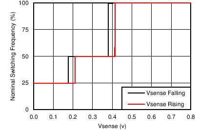
- 9.3.11 Frequency Shift
- 9.3.12 Reverse Overcurrent Protection
- 9.3.13 Synchronize Using the RT/CLK Pin
- 9.3.14 Power Good (PWRGD Pin)
- 9.3.15 Overvoltage Transient Protection (OVTP)
- 9.3.16 Thermal Shutdown
- 9.3.17 Small-Signal Model for Loop Response
- 9.3.18 Simple Small-Signal Model for Peak-Current Mode Control
- 9.3.19 Small-Signal Model for Frequency Compensation
- 9.4 Device Functional Modes
-
10Application and Implementation
- 10.1 Application Information
- 10.2
Typical Application
- 10.2.1 Design Requirements
- 10.2.2
Detailed Design Procedure
- 10.2.2.1 Selecting the Switching Frequency
- 10.2.2.2 Output Inductor Selection
- 10.2.2.3 Output Capacitor
- 10.2.2.4 Input Capacitor
- 10.2.2.5 Slow-Start Capacitor
- 10.2.2.6 Bootstrap Capacitor Selection
- 10.2.2.7 Output-Voltage and Feedback-Resistor Selection
- 10.2.2.8 Compensation
- 10.2.2.9 Power-Dissipation Estimate
- 10.2.3 Application Curves
- 11Power Supply Recommendations
- 12Layout
- 13器件和文档支持
- 14机械封装和可订购信息
8 Specifications
8.1 Absolute Maximum Ratings(1)
| MIN | MAX | UNIT | ||
|---|---|---|---|---|
| Input voltage | VIN | –0.3 | 7 | V |
| EN | –0.3 | 7 | ||
| BOOT | PH + 7 | |||
| VSENSE | –0.3 | 3 | ||
| COMP | –0.3 | 3 | ||
| PWRGD | –0.3 | 7 | ||
| SS/TR | –0.3 | 3 | ||
| RT/CLK | –0.3 | 7 | ||
| Output voltage | BOOT-PH | 7 | V | |
| PH | –0.6 | 7 | ||
| PH 10-ns transient | –2 | 10 | ||
| Source current | EN | 100 | µA | |
| RT/CLK | 100 | µA | ||
| Sink current | COMP | 100 | µA | |
| PWRGD | 10 | mA | ||
| SS/TR | 100 | µA | ||
| Temperature | TJ | –55 | 150 | °C |
(1) Stresses beyond those listed under Absolute Maximum Ratings may cause permanent damage to the device. These are stress ratings only, which do not imply functional operation of the device at these or any other conditions beyond those indicated under Recommended Operating Conditions. Exposure to absolute-maximum-rated conditions for extended periods may affect device reliability.
8.2 Handling Ratings
| MIN | MAX | UNIT | |||
|---|---|---|---|---|---|
| Tstg | Storage temperature range | –65 | 150 | °C | |
| V(ESD) | Electrostatic discharge | Human body model (HBM), per ANSI/ESDA/JEDEC JS-001, all pins(1) | –4000 | 4000 | V |
| Machine model (MM) | –200 | 200 | |||
| Charged device model (CDM), per JEDEC specification JESD22-C101, all pins(2) | –1500 | 1500 | |||
(1) JEDEC document JEP155 states that 500-V HBM allows safe manufacturing with a standard ESD control process.
(2) JEDEC document JEP157 states that 250-V CDM allows safe manufacturing with a standard ESD control process.
8.3 Recommended Operating Conditions
over operating free-air temperature range (unless otherwise noted)| MIN | NOM | MAX | UNIT | ||
|---|---|---|---|---|---|
| V(VIN) | Input voltage | 2.95 | 6 | V | |
| TA | Operating ambient temperature | –55 | 125 | °C | |
| TJ | Operating junction temperature | –55 | 150 | °C | |
8.4 Thermal Information
| THERMAL METRIC(1) | TPS57114-EP | UNIT | |
|---|---|---|---|
| RTE | |||
| 16 PINS | |||
| RθJA | Junction-to-ambient thermal resistance(2) | 44.4 | °C/W |
| RθJC(top) | Junction-to-case (top) thermal resistance(3) | 46.1 | |
| RθJB | Junction-to-board thermal resistance(4) | 16 | |
| ψJT | Junction-to-top characterization parameter(5) | 0.7 | |
| ψJB | Junction-to-board characterization parameter(6) | 16.9 | |
| RθJC(bot) | Junction-to-case (bottom) thermal resistance(7) | 4.6 | |
(1) For more information about traditional and new thermal metrics, see the IC Package Thermal Metrics application report, SPRA953.
(2) The junction-to-ambient thermal resistance under natural convection is obtained in a simulation on a JEDEC-standard, high-K board, as specified in JESD51-7, in an environment described in JESD51-2a.
(3) The junction-to-case (top) thermal resistance is obtained by simulating a cold plate test on the package top. No specific JEDEC-standard test exists, but a close description can be found in the ANSI SEMI standard G30-88.
(4) The junction-to-board thermal resistance is obtained by simulating in an environment with a ring cold plate fixture to control the PCB temperature, as described in JESD51-8.
(5) The junction-to-top characterization parameter, ψJT, estimates the junction temperature of a device in a real system and is extracted from the simulation data for obtaining θJA, using a procedure described in JESD51-2a (sections 6 and 7).
(6) The junction-to-board characterization parameter, ψJB, estimates the junction temperature of a device in a real system and is extracted from the simulation data for obtaining θJA , using a procedure described in JESD51-2a (sections 6 and 7).
(7) The junction-to-case (bottom) thermal resistance is obtained by simulating a cold plate test on the exposed (power) pad. No specific JEDEC standard test exists, but a close description can be found in the ANSI SEMI standard G30-88.
8.5 Electrical Characteristics
TJ = –55°C to 150°C, VIN = 2.95 to 6 V (unless otherwise noted)| PARAMETER | TEST CONDITIONS | MIN | TYP | MAX | UNIT |
|---|---|---|---|---|---|
| SUPPLY VOLTAGE (VIN PIN) | |||||
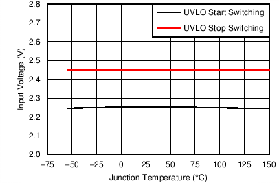
| Internal undervoltage-lockout threshold | VIN UVLO START | 2.28 | 2.5 | V | |
| VIN UVLO STOP | 2.45 | 2.6 | V | ||
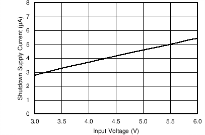
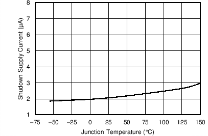
| Shutdown supply current | V(EN) = 0 V, 2.95 V ≤ V(VIN) ≤ 6 V | 5.5 | 15 | µA | |
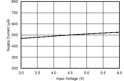
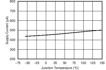
| Quiescent current – Iq | V(VSENSE) = 0.9 V, V(VIN) = 5 V, RT = 400 kΩ | 515 | 750 | µA | |
| ENABLE AND UVLO (EN PIN) | |||||
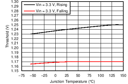
| Enable threshold | Rising | 1.25 | V | ||
| Falling | 1.18 | ||||
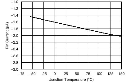
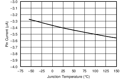
| Input current | Enable threshold + 50 mV | –3.2 | µA | ||
| Enable threshold – 50 mV | –1.65 | ||||
| VOLTAGE REFERENCE (VSENSE PIN) | |||||
| Voltage reference | 2.95 V ≤ V(VIN) ≤ 6 V, –55°C < TJ < 150°C | 0.79 | 0.8 | 0.81 | V |
| MOSFET | |||||
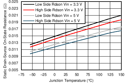
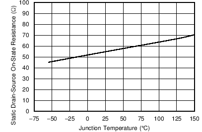
| High-side switch resistance | BOOT-PH = 5 V | 12 | 30 | mΩ | |
| BOOT-PH = 2.95 V | 16 | 30 | |||
| Low-side switch resistance | V(VIN) = 5 V | 13 | 30 | mΩ | |
| V(VIN) = 2.95 V | 17 | 30 | |||
| ERROR AMPLIFIER | |||||
| Input current | 2 | nA | |||
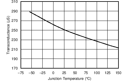
| Error-amplifier transconductance (gm) | –2 µA < I(COMP) < 2 µA, V(COMP) = 1 V | 245 | µS | ||
| Error-amplifier transconductance (gm) during slow start | –2 µA < I(COMP) < 2 µA, V(COMP) = 1 V, V(VSENSE) = 0.4 V |
79 | µS | ||
| Error-amplifier source and sink | V(COMP) = 1 V, 100-mV overdrive | ±20 | µA | ||
| COMP to Iswitch gm | 25 | S | |||
| CURRENT LIMIT | |||||
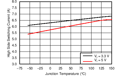
| Current-limit threshold | V(VIN) = 2.95 V, 25°C < TJ < 150°C | 5 | 6.4 | A | |
| TJ = –55°C | 4 | ||||
| V(VIN) = 6 V, 25°C < TJ < 150°C | 4.4 | 5.56 | |||
| TJ = –55°C | 4 | ||||
| THERMAL SHUTDOWN | |||||
| Thermal shutdown | 168 | °C | |||
| Hysteresis | 20 | °C | |||
| TIMING RESISTOR AND EXTERNAL CLOCK (RT/CLK PIN) | |||||
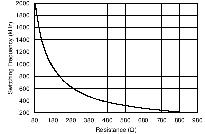
| Switching frequency range using RT mode | 200 | 2000 | kHz | ||
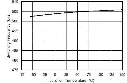
| Switching frequency | R(RT/CLK) = 400 kΩ | 400 | 500 | 600 | kHz |
| Switching frequency range using CLK mode | 300 | 2000 | kHz | ||
| Minimum CLK pulse duration | 80 | ns | |||
| RT/CLK voltage | R(RT/CLK) = 400 kΩ | 0.5 | V | ||
| RT/CLK high threshold | 1.6 | 2.5 | V | ||
| RT/CLK low threshold | 0.4 | 0.6 | V | ||
| RT/CLK falling edge to PH rising edge delay | Measure at 500 kHz with RT resistor in series | 90 | ns | ||
| PLL lock in time | Measure at 500 kHz | 42 | µs | ||
| PH (PH PIN) | |||||
| Minimum on-time | Measured at 50% points on PH, IOUT = 3.5 A | 75 | ns | ||
| Measured at 50% points on PH, V(VIN) = 6 V, IOUT = 0 A |
120 | ||||
| Minimum off-time | Prior to skipping off pulses, BOOT-PH = 2.95 V, IOUT = 3.5 A |
60 | ns | ||
| Rise time | V(VIN) = 6 V, 3.5 A | 2.25 | V/ns | ||
| Fall time | 2 | ||||
| BOOT (BOOT PIN) | |||||
| BOOT charge resistance | V(VIN) = 5 V | 16 | Ω | ||
| BOOT-PH UVLO | V(VIN) = 2.95 V | 2.1 | V | ||
| SLOW START AND TRACKING (SS/TR PIN) | |||||
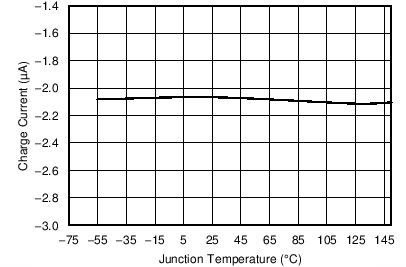
| Charge current | V(SS/TR) = 0.4 V | 2 | µA | ||
| SS/TR to VSENSE matching | V(SS/TR) = 0.4 V | 54 | mV | ||
| SS/TR to reference crossover | 98% normal | 1.1 | V | ||
| SS/TR discharge voltage (overload) | V(VSENSE) = 0 V | 60 | mV | ||
| SS/TR discharge current (overload) | V(VSENSE) = 0 V, V(SS/TR) = 0.4 V | 350 | µA | ||
| SS discharge current (UVLO, EN, thermal fault) | V(VIN) = 5 V, V(SS) = 0.5 V | 1.9 | mA | ||
| POWER-GOOD (PWRGD PIN) | |||||
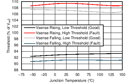
| VSENSE threshold | V(VSENSE) falling (fault) | 91 | %V(VREF) | ||
| V(VSENSE) rising (good) | 93 | ||||
| V(VSENSE) rising (fault) | 109 | ||||
| V(VSENSE) falling (good) | 107 | ||||
| Hysteresis | V(VSENSE) falling | 2 | %V(VREF) | ||
| Output high leakage | V(VSENSE) = V(VREF), V(PWRGD) = 5.5 V | 7 | nA | ||
| On-resistance | 56 | 100 | Ω | ||
| Output low | I(PWRGD) = 3 mA | 0.3 | V | ||
| Minimum VIN for valid output | V(PWRGD) < 0.5 V at 100 µA | 0.650 | 1.5 | V | |
1. See data sheet for absolute maximum and minimum recommended operating conditions.
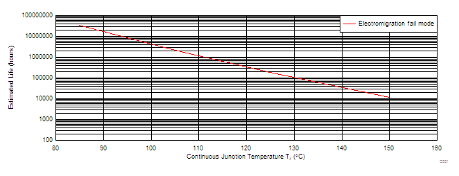
2. Silicon operating life design goal is 10 years at 105°C junction temperature (does not include package interconnect life).
3. Enhanced plastic product disclaimer applies.
Figure 1. TPS57114-EP Derating Chart
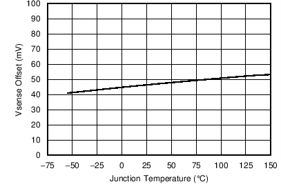
8.6 Typical Characteristics
| VIN = 3 V | ||
| VIN = 5 V | VEN = Threshold –50 mV | |
| TJ = 25°C | ||
| TJ = 25°C | ||
| VIN = 5 V | ||
| RT = 400 kΩ | VIN = 5 V | |
| VIN = 3.3 V | ||
| VIN = 3.3 V | ||
| VIN = 5 V | VEN = Threshold +50 mV | |
| VIN = 5 V | ||
| VIN = 3.3 V | ||
| VIN = 3.3 V | ||
| VIN = 5 V | SS = 0.4 V | |