ZHCSCN2 July 2014 TPS57114-EP
PRODUCTION DATA.
- 1 特性
- 2 应用范围
- 3 说明
- 4 简化电路原理图
- 5 修订历史记录
- 6 说明(续)
- 7 Pin Configuration and Functions
- 8 Specifications
-
9 Detailed Description
- 9.1 Overview
- 9.2 Functional Block Diagram
- 9.3
Feature Description
- 9.3.1 Fixed-Frequency Pwm Control
- 9.3.2 Slope Compensation and Output Current
- 9.3.3 Bootstrap Voltage (Boot) and Low-Dropout Operation
- 9.3.4 Error Amplifier
- 9.3.5 Voltage Reference
- 9.3.6 Adjusting the Output Voltage
- 9.3.7 Enable Functionality and Adjusting UVLO
- 9.3.8 Slow-Start or Tracking Pin
- 9.3.9 Constant Switching Frequency and Timing Resistor (RT/CLK Pin)
- 9.3.10 Overcurrent Protection
- 9.3.11 Frequency Shift
- 9.3.12 Reverse Overcurrent Protection
- 9.3.13 Synchronize Using the RT/CLK Pin
- 9.3.14 Power Good (PWRGD Pin)
- 9.3.15 Overvoltage Transient Protection (OVTP)
- 9.3.16 Thermal Shutdown
- 9.3.17 Small-Signal Model for Loop Response
- 9.3.18 Simple Small-Signal Model for Peak-Current Mode Control
- 9.3.19 Small-Signal Model for Frequency Compensation
- 9.4 Device Functional Modes
-
10Application and Implementation
- 10.1 Application Information
- 10.2
Typical Application
- 10.2.1 Design Requirements
- 10.2.2
Detailed Design Procedure
- 10.2.2.1 Selecting the Switching Frequency
- 10.2.2.2 Output Inductor Selection
- 10.2.2.3 Output Capacitor
- 10.2.2.4 Input Capacitor
- 10.2.2.5 Slow-Start Capacitor
- 10.2.2.6 Bootstrap Capacitor Selection
- 10.2.2.7 Output-Voltage and Feedback-Resistor Selection
- 10.2.2.8 Compensation
- 10.2.2.9 Power-Dissipation Estimate
- 10.2.3 Application Curves
- 11Power Supply Recommendations
- 12Layout
- 13器件和文档支持
- 14机械封装和可订购信息
12 Layout
12.1 Layout Guidelines
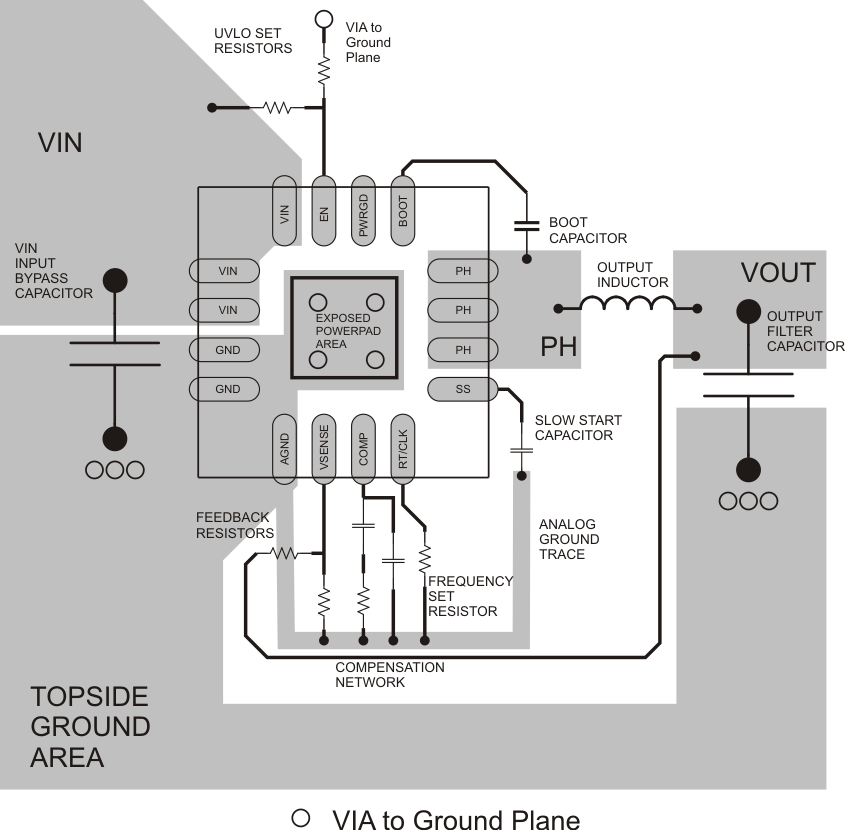
Layout is a critical portion of good power-supply design. There are several signal paths that conduct fast-changing currents or voltages that can interact with stray inductance or parasitic capacitance to generate noise or degrade the power-supply performance. Take care to minimize the loop area formed by the bypass capacitor connections and the VIN pins. See Layout Example for a PCB layout example. Tie the GND pins and AGND pin directly to the thermal pad under the IC. Connect the thermal pad to any internal PCB ground planes using multiple vias directly under the IC. Use additional vias to connect the top-side ground area to the internal planes near the input and output capacitors. For operation at full-rated load, the top-side ground area along with any additional internal ground planes must provide adequate heat dissipating area.
Locate the input bypass capacitor as close to the IC as possible. Route the PH pin to the output inductor. Because the PH connection is the switching node, locate the output inductor close to the PH pins and minimize the area of the PCB conductor to prevent excessive capacitive coupling. Also, locate the boot capacitor close to the device. Connect the sensitive analog ground connections for the feedback voltage divider, compensation components, slow-start capacitor, and frequency-set resistor to a separate analog ground trace as shown. The RT/CLK pin is particularly sensitive to noise, so locate the RT resistor as close as possible to the IC and connect it with minimal lengths of trace. Place the additional external components approximately as shown. It may be possible to obtain acceptable performance with alternative PCB layout. However, this layout, meant as a guideline, produces good results.
12.2 Layout Example