ZHCSCN2 July 2014 TPS57114-EP
PRODUCTION DATA.
- 1 特性
- 2 应用范围
- 3 说明
- 4 简化电路原理图
- 5 修订历史记录
- 6 说明(续)
- 7 Pin Configuration and Functions
- 8 Specifications
-
9 Detailed Description
- 9.1 Overview
- 9.2 Functional Block Diagram
- 9.3
Feature Description
- 9.3.1 Fixed-Frequency Pwm Control
- 9.3.2 Slope Compensation and Output Current
- 9.3.3 Bootstrap Voltage (Boot) and Low-Dropout Operation
- 9.3.4 Error Amplifier
- 9.3.5 Voltage Reference
- 9.3.6 Adjusting the Output Voltage
- 9.3.7 Enable Functionality and Adjusting UVLO
- 9.3.8 Slow-Start or Tracking Pin
- 9.3.9 Constant Switching Frequency and Timing Resistor (RT/CLK Pin)
- 9.3.10 Overcurrent Protection
- 9.3.11 Frequency Shift
- 9.3.12 Reverse Overcurrent Protection
- 9.3.13 Synchronize Using the RT/CLK Pin
- 9.3.14 Power Good (PWRGD Pin)
- 9.3.15 Overvoltage Transient Protection (OVTP)
- 9.3.16 Thermal Shutdown
- 9.3.17 Small-Signal Model for Loop Response
- 9.3.18 Simple Small-Signal Model for Peak-Current Mode Control
- 9.3.19 Small-Signal Model for Frequency Compensation
- 9.4 Device Functional Modes
-
10Application and Implementation
- 10.1 Application Information
- 10.2
Typical Application
- 10.2.1 Design Requirements
- 10.2.2
Detailed Design Procedure
- 10.2.2.1 Selecting the Switching Frequency
- 10.2.2.2 Output Inductor Selection
- 10.2.2.3 Output Capacitor
- 10.2.2.4 Input Capacitor
- 10.2.2.5 Slow-Start Capacitor
- 10.2.2.6 Bootstrap Capacitor Selection
- 10.2.2.7 Output-Voltage and Feedback-Resistor Selection
- 10.2.2.8 Compensation
- 10.2.2.9 Power-Dissipation Estimate
- 10.2.3 Application Curves
- 11Power Supply Recommendations
- 12Layout
- 13器件和文档支持
- 14机械封装和可订购信息
10 Application and Implementation
10.1 Application Information
10.1.1 Sequencing
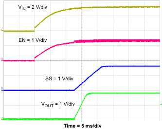
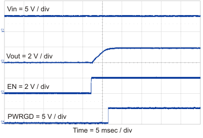
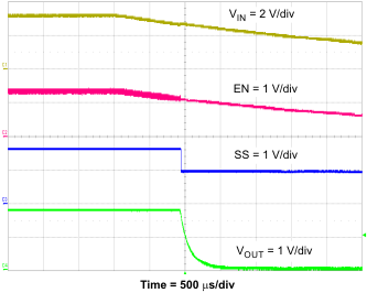
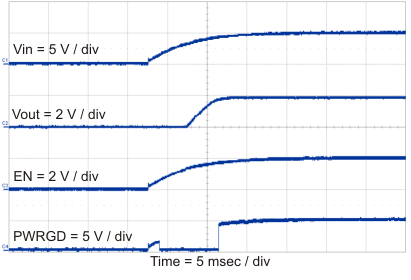
The user can implement many of the common power-supply sequencing methods using the SS/TR, EN, and PWRGD pins. Implement the sequential method by using an open-drain or collector output of the power-on-reset pin of another device. Figure 30 shows the sequential method. Coupling power-good to the EN pin on the TPS57114-EP enables the second power supply after the primary supply reaches regulation.
The user can accomplish ratiometric start-up by connecting the SS/TR pins together. The regulator outputs ramp up and reach regulation at the same time. When calculating the slow-start time, double the pullup current source in Equation 4. Figure 32 shows the ratiometric method.
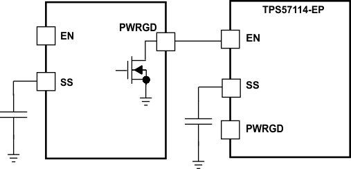
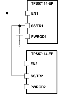
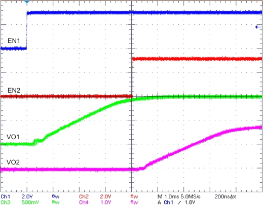 Figure 31. Sequential Start-Up Using EN and PWRGD
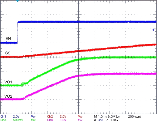
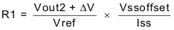
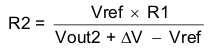
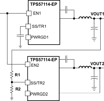
The user can implement ratiometric and simultaneous power-supply sequencing by connecting the resistor network of R1 and R2 shown in Figure 34 to the output of the power supply that requires tracking, or to another voltage reference source. Using Equation 18 and Equation 19 allows calculation of the tracking resistors to initiate the Vout2 slightly before, after, or at the same time as Vout1. Equation 20 is the voltage difference between Vout1 and Vout2. The ΔV variable is 0 V for simultaneous sequencing. To minimize the effect of the inherent SS/TR-to-VSENSE offset (Vssoffset) in the slow-start circuit and the offset created by the pullup current source (Iss) and tracking resistors, the equations include Vssoffset and Iss as variables. To design a ratiometric start-up in which the Vout2 voltage is slightly greater than the Vout1 voltage when Vout2 reaches regulation, use a negative number in Equation 18 through Equation 20 for ΔV. Equation 20 results in a positive number for applications in which Vout2 is slightly lower than Vout1 when achieving Vout2 regulation. The requirement to pull the SS/TR pin below 60 mV before starting after an EN, UVLO, or thermal shutdown fault necessitates careful selection of the tracking resistors to ensure the device can restart after a fault. Make sure the calculated R1 value from Equation 18 is greater than the value calculated in Equation 21 to ensure the device can recover from a fault. As the SS/TR voltage becomes more than 85% of the nominal reference voltage, Vssoffset becomes larger as the slow-start circuits gradually hand off the regulation reference to the internal voltage reference. The SS/TR pin voltage must be greater than 1.1 V for a complete handoff to the internal voltage reference, as shown in Figure 33.
10.2 Typical Application
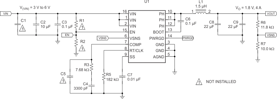 Figure 36. High-Frequency, 1.8-V Output Power-Supply Design With Adjusted UVLO
10.2.1 Design Requirements
This example details the design of a high-frequency switching regulator using ceramic output capacitors. This design is available as the HPA375 evaluation module (EVM). To start the design process, it is necessary to know a few parameters. Determination of these parameters typically occurs at the system level. For this example, start with the following known parameters:
Table 1. Design Parameters
| DESIGN PARAMETER | EXAMPLE VALUE |
|---|---|
| Output voltage | 1.8 V |
| Transient response, 1- to 2-A load step | ΔVout = 5% |
| Maximum output current | 3.5 A |
| Input voltage | 5 V nominal, 3 to 5 V |
| Output-voltage ripple | <30 mVp-p |
| Switching frequency (ƒSW) | 1000 kHz |
10.2.2 Detailed Design Procedure
10.2.2.1 Selecting the Switching Frequency
The first step is to decide on a switching frequency for the regulator. Typically, the user wants to choose the highest switching frequency possible, because this produces the smallest solution size. The high switching frequency allows for lower-valued inductors and smaller output capacitors compared to a power supply that switches at a lower frequency. However, the highest switching frequency causes extra switching losses, which hurt the performance of the converter. The converter is capable of running from 300 kHz to 2 MHz. Unless a small solution size is the ultimate goal, select a moderate switching frequency of 1 MHz to achieve both a small solution size and high-efficiency operation. Using Equation 5, calculate R5 to be 180 kΩ. Choose a standard 1% 182-kΩ value for the design.
10.2.2.2 Output Inductor Selection
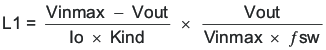
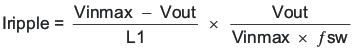
The inductor selected works for the entire TPS57114-EP input-voltage range. To calculate the value of the output inductor, use Equation 22. KIND is a coefficient that represents the amount of inductor ripple current relative to the maximum output current. The output capacitor filters the inductor ripple current. Therefore, choosing high inductor ripple currents impacts the selection of the output capacitor, because the output capacitor must have a ripple-current rating equal to or greater than the inductor ripple current. In general, the inductor ripple value is at the discretion of the designer; however, KIND is normally from 0.1 to 0.3 for the majority of applications.
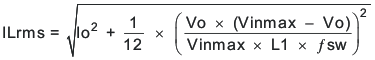
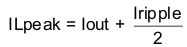
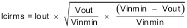
For this design example, use KIND = 0.3, which results in a calculated inductor value of 1.36 µH. For this design, choose the nearest standard value: 1.5 µH. For the output-filter inductor, it is important not to exceed the rms-current and saturation-current ratings. Find the rms and peak inductor current using Equation 24 and Equation 25.
For this design, the rms inductor current is 4 A and the peak inductor current is 4.6 A. The chosen inductor is a Coilcraft XLA4020-152ME_ or equivalent. It has a saturation current rating of 9.6 A and an rms current rating of 7.5 A.
The current flowing through the inductor is the inductor ripple current plus the output current. During power-up, faults, or transient load conditions, the inductor current can increase above the calculated peak inductor-current level calculated previously. In transient conditions, the inductor current can increase up to the switch-current limit of the device. For this reason, the most conservative approach is to specify an inductor with a saturation current rating equal to or greater than the switch-current limit rather than the peak inductor current.
10.2.2.3 Output Capacitor
To select the value of the output capacitor, use three primary considerations. The output capacitor determines the modulator pole, the output-voltage ripple, and how the regulator responds to a large change in load current. Base the output-capacitance selection on the most stringent of these three criteria.
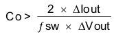
The desired response to a large change in the load current is the first criterion. The output capacitor must supply the load with current when the regulator cannot. This situation would occur if there are desired hold-up times for the regulator where the output capacitor must hold the output voltage above a certain level for a specified amount of time after removal of the input power. The regulator is temporarily not able to supply sufficient output current if there is a large, fast increase in the current needs of the load, such as transitioning from no load to a full load. The regulator usually requires two or more clock cycles for the control loop to detect the change in load current and output voltage and adjust the duty cycle to react to the change. The output capacitor size must be capable of supplying the extra current to the load until the control loop responds to the load change. The output capacitance must be large enough to supply the difference in current for two clock cycles while only allowing a tolerable amount of droop in the output voltage. Equation 26 shows the minimum output capacitance necessary to accomplish this.
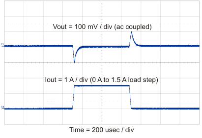
For this example, the transient load response is specified as a 5% change in Vout for a load step from 0 A (no load) to 1.5 A (50% load). For this example, ΔIout = 1.5 – 0 = 1.5 A and ΔVout= 0.05 × 1.8 = 0.09 V. Using these numbers gives a minimum capacitance of 33 µF. This value does not take the ESR of the output capacitor into account in the output voltage change. For ceramic capacitors, the ESR is usually small enough to ignore in this calculation.
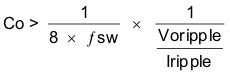
Equation 27 calculates the minimum output capacitance needed to meet the output-voltage ripple specification. In this case, the maximum output voltage ripple is 30 mV. Under this requirement, Equation 27 yields 2.3 µF.
where
- ΔIout is the change in output current
- ƒsw is the regulator switching frequency
- ΔVout is the allowable change in the output voltage
where
- ƒsw is the switching frequency
- Voripple is the maximum allowable output-voltage ripple
- Iripple is the inductor ripple current
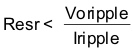
Equation 28 calculates the maximum ESR an output capacitor can have to meet the output-voltage ripple specification. Equation 28 indicates the ESR should be less than 55 mΩ. In this case, the ESR of the ceramic capacitor is much less than 55 mΩ.
Factoring in additional capacitance deratings for aging, temperature, and DC bias increases this minimum value. This example uses two 22-µF, 10-V X5R ceramic capacitors with 3 mΩ of ESR.
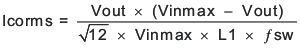
Capacitors generally have limits to the amount of ripple current they can handle without failing or producing excess heat. Specify an output capacitor that can support the inductor ripple current. Some capacitor data sheets specify the root-mean-square (rms) value of the maximum ripple current. Use Equation 29 to calculate the rms ripple current that the output capacitor must support. For this application, Equation 29 yields 333 mA.
10.2.2.4 Input Capacitor
The TPS57114-EP requires a high-quality ceramic, type X5R or X7R, input decoupling capacitor with at least 4.7 µF of effective capacitance, and in some applications a bulk capacitance. The effective capacitance includes any DC-bias effects. The voltage rating of the input capacitor must be greater than the maximum input voltage. The capacitor must also have a ripple-current rating greater than the maximum input-current ripple of the TPS57114-EP. Calculate the input ripple current using Equation 30.
The value of a ceramic capacitor varies significantly over temperature and the amount of DC bias applied to the capacitor. The capacitance variations due to temperature can be minimized by selecting a dielectric material that is stable over temperature. The dielectrics are usually selected for power regulator capacitors are X5R and X7R ceramic because they have a high capacitance-to-volume ratio and are fairly stable over temperature. Also select the output capacitor with the DC bias taken into account. The capacitance value of a capacitor decreases as the DC bias across a capacitor increases.
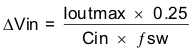
This design example requires a ceramic capacitor with at least a 10-V voltage rating to support the maximum input voltage. The selections for this example are one 10-µF and one 0.1-µF 10-V capacitor in parallel. The input capacitance value determines the input ripple voltage of the regulator. Calculate the input voltage ripple using Equation 31. Using the design example values, Ioutmax = 4 A, Cin = 10 µF, and ƒsw = 1 MHz, yields an input-voltage ripple of 100 mV and an rms input-ripple current of 1.96 A.
10.2.2.5 Slow-Start Capacitor
The slow-start capacitor determines the minimum amount of time it takes for the output voltage to reach its nominal programmed value during power up. Slow start is useful if a load requires a controlled rate of voltage slew. Slow start is also used if the output capacitance is large and would require large amounts of current to charge the capacitor quickly to the output-voltage level. The large currents necessary to charge the capacitor may make the TPS57114-EP reach the current limit, or excessive current draw from the input power supply may cause the input voltage rail to sag. Limiting the output-voltage slew rate solves both of these problems.
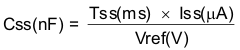
Calculate the slow-start capacitor value using Equation 32. For the example circuit, the slow-start time is not too critical because the output capacitor value is 44 µF, which does not require much current to charge to 1.8 V. The example circuit has the slow-start time set to an arbitrary value of 4 ms, which requires a 10-nF capacitor. In TPS57114-EP, Iss is 2.2 µA and Vref is 0.8 V.
10.2.2.6 Bootstrap Capacitor Selection
Connect a 0.1-µF ceramic capacitor between the BOOT and PH pins for proper operation. TI recommends using a ceramic capacitor with X5R or better-grade dielectric. The capacitor should have a 10-V, or higher, voltage rating.
10.2.2.7 Output-Voltage and Feedback-Resistor Selection
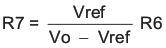
For the design example, the selection for R6 is 100 kΩ. Using Equation 33, calculate R7 as 80 kΩ. The nearest standard 1% resistor is 80.5 kΩ.
Due to the internal design of the TPS57114-EP, a minimum output voltage limit exists for any given input voltage. The output voltage can never be lower than the internal voltage reference of 0.8 V. Above 0.8 V, an output voltage limit may exist due to the minimum controllable on-time. In this case, Equation 34 gives the minimum output voltage.

where
- Voutmin = Minimum achievable output voltage
- Ontimemin = Minimum controllable on-time (65 ns, typical; 120 ns, no load)
- Fsmax = Maximum switching frequency, including tolerance
- Vinmax = Maximum input voltage
- Ioutmin = Minimum load current
- RDS = Minimum high-side MOSFET on-resistance (15 to 19 mΩ)
- RL = Series resistance of output inductor
There is also a maximum achievable output voltage, which is limited by the minimum off-time. Equation 35 gives the maximum output voltage

where
- Voutmax = Maximum achievable output voltage
- Offtimeman = Maximum off-time (60 ns, typical)
- Fsmax = Maximum switching frequency, including tolerance
- Vinmin = Minimum input voltage
- Ioutmax = Maximum load current
- RDS = Maximum high-side MOSFET on-resistance (19 to 30 mΩ)
- RL = Series resistance of output inductor
10.2.2.8 Compensation
Several industry techniques are used to compensate DC-DC regulators. The method presented here is easy to calculate and yields high phase margins. For most conditions, the regulator has a phase margin between 60° and 90°. The method presented here ignores the effects of the slope compensation that is internal to the TPS57114-EP. Because of ignoring the slope compensation, the actual crossover frequency is usually lower than the crossover frequency used in the calculations. Use SwitcherPro software for a more-accurate design.
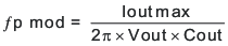
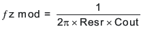
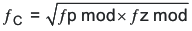
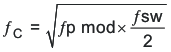
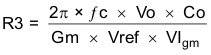
To get started, calculate the modulator pole, ƒpmod, and the ESR zero, ƒz1, using Equation 36 and Equation 37. For Cout, derating the capacitor is not necessary, as the 1.8-V output is a small percentage of the 10-V capacitor rating. If the output is a high percentage of the capacitor rating, use the manufacturer information for the capacitor to derate the capacitor value. Use Equation 38 and Equation 39 to estimate a starting point for the crossover frequency, ƒc. For the example design, ƒpmod is 6.03 kHz and ƒzmod is 1210 kHz. Equation 38 is the geometric mean of the modulator pole and the ESR zero, and Equation 39 is the mean of the modulator pole and the switching frequency. Equation 38 yields 85.3 kHz and Equation 39 gives 54.9 kHz. Use the lower value of Equation 38 or Equation 39 as the approximate crossover frequency. For this example, ƒc is 56 kHz. Next, calculate the compensation components. Use a resistor in series with a capacitor to create a compensating zero. A capacitor in parallel with these two components forms the compensating pole (if needed).
The compensation design takes the following steps:
- Set up the anticipated crossover frequency. Use Equation 40 to calculate the resistor value for the compensation network. In this example, the anticipated crossover frequency (ƒc) is 56 kHz. The power-stage gain (gmps) is 25 S, and the error-amplifier gain (gmea) is 245 µS.
- Place compensation zero at the pole formed by the load resistor and the output capacitor. Calculate the capacitor for the compensation network using Equation 41.
- The user can add an additional pole to attenuate high-frequency noise. In this application, it is not necessary to add it.
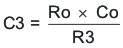
From the preceding procedure, the compensation network includes a 7.68-kΩ resistor and a 3300-pF capacitor.
10.2.2.9 Power-Dissipation Estimate
The following formulas show how to estimate the IC power dissipation under continuous-conduction mode (CCM) operation. The power dissipation of the IC (Ptot) includes conduction loss (Pcon), dead-time loss (Pd), switching loss (Psw), gate-drive loss (Pgd), and supply-current loss (Pq).
where:
- IO is the output current (A)
- rDS(on)_Temp is the on-resistance of the high-side MOSFET at a given temperature (Ω)
- Vin is the input voltage (V)
- ƒsw is the switching frequency (Hz)
So
For a given TA,
For a given TJMAX = 150°C,
where:
- Ptot is the total device power dissipation (W)
- TA is the ambient temperature (°C)
- TJ is the junction temperature (°C)
- Rth is the thermal resistance of the package (°C/W)
- TJMAX is maximum junction temperature (°C)
- TAMAX is maximum ambient temperature (°C)
Additional power losses in the regulator circuit occur due to the inductor ac and dc losses and trace resistance that impact the overall efficiency of the regulator.
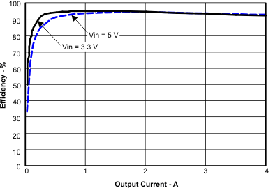
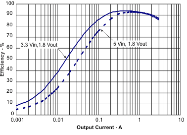
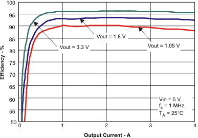
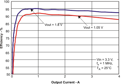
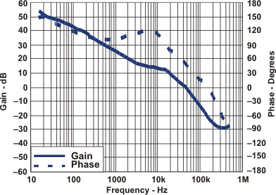
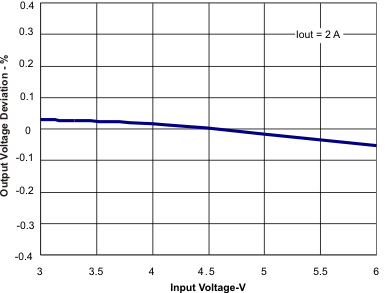
10.2.3 Application Curves