ZHCS920B May 2012 – April 2021 TPS54525
PRODUCTION DATA
- 1 特性
- 2 应用
- 3 说明
- 4 Revision History
- 5 Pin Configuration and Functions
- 6 Specifications
- 7 Detailed Description
- 8 Application and Implementation
- 9 Power Supply Recommendations
- 10Layout
- 11Device and Documentation Support
封装选项
机械数据 (封装 | 引脚)
- PWP|14
散热焊盘机械数据 (封装 | 引脚)
- PWP|14
订购信息
8.2.2.3 Output Filter Selection
The output filter used with the TPS54525 is an LC circuit. This LC filter has double pole at:
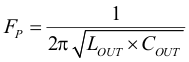
At low frequencies, the overall loop gain is set by the output set-point resistor divider network and the internal gain of the TPS54525. The low frequency phase is 180 degrees. At the output filter pole frequency, the gain rolls off at a -40 dB per decade rate and the phase drops rapidly. D-CAP2™ introduces a high frequency zero that reduces the gain roll off to -20 dB per decade and increases the phase to 90 degrees one decade above the zero frequency. The inductor and capacitor selected for the output filter must be selected so that the double pole of Equation 3 is located below the high frequency zero but close enough that the phase boost provided be the high frequency zero provides adequate phase margin for a stable circuit. To meet this requirement use the values recommended in Table 8-2
| Output Voltage (V) | R1 (kΩ) | R2 (kΩ) | C4 (pF)(1) | L1 (µH) | C8 + C9 (µF) |
|---|---|---|---|---|---|
| 1 | 6.81 | 22.1 | 1.0 - 1.5 | 22 - 68 | |
| 1.05 | 8.25 | 22.1 | 1.0 - 1.5 | 22 - 68 | |
| 1.2 | 12.7 | 22.1 | 1.0 - 1.5 | 22 - 68 | |
| 1.5 | 21.5 | 22.1 | 1.5 | 22 - 68 | |
| 1.8 | 30.1 | 22.1 | 5 - 22 | 1.5 | 22 - 68 |
| 2.5 | 49.9 | 22.1 | 5 - 22 | 2.2 | 22 - 68 |
| 3.3 | 73.2 | 22.1 | 5 - 22 | 2.2 | 22 - 68 |
| 5 | 124 | 22.1 | 5 - 22 | 3.3 | 22 - 68 |
For higher output voltages at or above 1.8 V, additional phase boost can be achieved by adding a feed forward capacitor (C4) in parallel with R1.
Since the DC gain is dependent on the output voltage, the required inductor value will increase as the output voltage increases. For higher output voltages at or above 1.8 V, additional phase boost can be achieved by adding a feed forward capacitor (C4) in parallel with R1
The inductor peak-to-peak ripple current, peak current and RMS current are calculated using Equation 4, Equation 5 and Equation 6. The inductor saturation current rating must be greater than the calculated peak current and the RMS or heating current rating must be greater than the calculated RMS current. Use 650 kHz for fSW.
Use 650 kHz for fSW. Make sure the chosen inductor is rated for the peak current of Equation 5 and the RMS current of Equation 6.
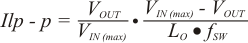
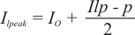
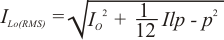
For this design example, the calculated peak current is 6.01 A and the calculated RMS current is 5.5 A. The inductor used is a TDK SPM6530-1R5M100 with a peak current rating of 11.5 A and an RMS current rating of 11 A.
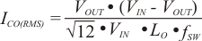
The capacitor value and ESR determines the amount of output voltage ripple. The TPS54525 is intended for use with ceramic or other low ESR capacitors. Recommended values range from 22uF to 68uF. Use Equation 7 to determine the required RMS current rating for the output capacitor.
For this design two TDK C3216X5R0J226M 22uF output capacitors are used. The typical ESR is 2 mΩ each. The calculated RMS current is 0.284 A and each output capacitor is rated for 4A.