ZHCS920B May 2012 – April 2021 TPS54525
PRODUCTION DATA
- 1 特性
- 2 应用
- 3 说明
- 4 Revision History
- 5 Pin Configuration and Functions
- 6 Specifications
- 7 Detailed Description
- 8 Application and Implementation
- 9 Power Supply Recommendations
- 10Layout
- 11Device and Documentation Support
封装选项
机械数据 (封装 | 引脚)
- PWP|14
散热焊盘机械数据 (封装 | 引脚)
- PWP|14
订购信息
5 Pin Configuration and Functions
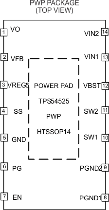
Table 5-1 Pin Functions
| PIN | DESCRIPTION | |
|---|---|---|
| NAME | NO. | |
| VO | 1 | Connect to output of converter. This pin is used for output discharge function. |
| VFB | 2 | Converter feedback input. Connect to output voltage with feedback resistor divider. |
| VREG5 | 3 | 5.5 V power supply output. A capacitor (typical 1 µF) should be connected to GND. VREG5 is not active when EN is low. |
| SS | 4 | Soft-start control. An external capacitor should be connected to GND. |
| GND | 5 | Signal ground pin |
| PG | 6 | Open drain power good output |
| EN | 7 | Enable control input. EN is active high and must be pulled up to enable the device. |
| PGND1, PGND2 | 8, 9 | Ground returns for low-side MOSFET. Also serve as inputs of current comparators. Connect PGND and GND strongly together near the IC. |
| SW1, SW2 | 10, 11 | Switch node connection between high-side NFET and low-side NFET. Also serve as inputs to current comparators. |
| VBST | 12 | Supply input for high-side NFET gate driver (boost terminal). Connect capacitor from this pin to respective SW1, SW2 terminals. An internal PN diode is connected between VREG5 to VBST pin. |
| VIN1, VIN2 | 13, 14 | Power input and connected to high side NFET drain. Supply input for 5-V internal linear regulator for the control circuitry. |
| PowerPAD™ | Back side | Thermal pad of the package. Must be soldered to achieve appropriate dissipation. Should be connected to PGND. |