ZHCSI26C August 2010 – April 2018 TPS54320
PRODUCTION DATA.
- 1 特性
- 2 应用
- 3 说明
- 4 修订历史记录
- 5 Pin Configuration and Functions
- 6 Specifications
-
7 Detailed Description
- 7.1 Overview
- 7.2 Functional Block Diagram
- 7.3
Feature Description
- 7.3.1 Fixed Frequency PWM Control
- 7.3.2 Continuous Current Mode Operation (CCM)
- 7.3.3 VIN and Power VIN Pins (VIN and PVIN)
- 7.3.4 Voltage Reference
- 7.3.5 Adjusting the Output Voltage
- 7.3.6 Safe Start-up into Prebiased Outputs
- 7.3.7 Error Amplifier
- 7.3.8 Slope Compensation
- 7.3.9 Enable and Adjusting UVLO
- 7.3.10 Slow Start (SS/TR)
- 7.3.11 Power Good (PWRGD)
- 7.3.12 Bootstrap Voltage (BOOT) and Low Dropout Operation
- 7.3.13 Sequencing (SS/TR)
- 7.3.14 Output Overvoltage Protection (OVP)
- 7.3.15 Overcurrent Protection
- 7.3.16 Thermal Shutdown
- 7.3.17 Small Signal Model for Loop Response
- 7.3.18 Simple Small Signal Model for Peak Current Mode Control
- 7.3.19 Small Signal Model for Frequency Compensation
- 7.4 Device Functional Modes
-
8 Application and Implementation
- 8.1 Application Information
- 8.2
Typical Application
- 8.2.1 Design Requirements
- 8.2.2
Detailed Design Procedure
- 8.2.2.1 Custom Design With WEBENCH® Tools
- 8.2.2.2 Operating Frequency
- 8.2.2.3 Output Inductor Selection
- 8.2.2.4 Output Capacitor Selection
- 8.2.2.5 Input Capacitor Selection
- 8.2.2.6 Slow-Start Capacitor Selection
- 8.2.2.7 Bootstrap Capacitor Selection
- 8.2.2.8 UVLO Set Point
- 8.2.2.9 Output Voltage Feedback Resistor Selection
- 8.2.2.10 Compensation Component Selection
- 8.2.3 Application Curves
- 9 Power Supply Recommendations
- 10Layout
- 11器件和文档支持
- 12机械、封装和可订购信息
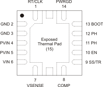
5 Pin Configuration and Functions
RHL Package
14-Pin VQFN
Top View

Pin Functions
| PIN | DESCRIPTION | |
|---|---|---|
| NAME | NO. | |
| RT/CLK | 1 | Automatically selects between RT mode and CLK mode. An external timing resistor adjusts the switching frequency of the device; In CLK mode, the device synchronizes to an external clock. |
| GND | 2 | Return for control circuitry and low-side power MOSFET. |
| 3 | ||
| PVIN | 4 | Power input. Supplies the power switches of the power converter. |
| 5 | ||
| VIN | 6 | Supplies the control circuitry of the power converter. |
| VSENSE | 7 | Inverting input of the gm error amplifier. |
| COMP | 8 | Error amplifier output, and input to the output switch current comparator. Connect frequency compensation to this pin. |
| SS/TR | 9 | Slow-start and tracking. An external capacitor connected to this pin sets the internal voltage reference rise time. The voltage on this pin overrides the internal reference. It can be used for tracking and sequencing. |
| EN | 10 | Enable pin. Float to enable. Adjust the input undervoltage lockout with two resistors. |
| PH | 11 | The switch node |
| 12 | ||
| BOOT | 13 | A bootstrap cap is required between BOOT and PH. The voltage on this cap carries the gate drive voltage for the high-side MOSFET. |
| PWRGD | 14 | Open-drain Power Good fault pin. Asserts low due to thermal shutdown, undervoltage, overvoltage, EN shutdown, or during slow start. |
| Exposed thermal PAD | 15 | Thermal pad of the package and signal ground. It must be soldered down for proper operation. |