ZHCSI26C August   2010  – April 2018 TPS54320

PRODUCTION DATA.  

  1. 特性
  2. 应用
  3. 说明
    1.     Device Images
      1.      简化原理图
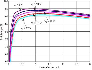
      2.      效率与负载电流间的关系
  4. 修订历史记录
  5. Pin Configuration and Functions
    1.     Pin Functions
  6. Specifications
    1. 6.1 Absolute Maximum Ratings
    2. 6.2 ESD Ratings
    3. 6.3 Recommended Operating Conditions
    4. 6.4 Thermal Information
    5. 6.5 Electrical Characteristics
    6. 6.6 Typical Characteristics
  7. Detailed Description
    1. 7.1 Overview
    2. 7.2 Functional Block Diagram
    3. 7.3 Feature Description
      1. 7.3.1  Fixed Frequency PWM Control
      2. 7.3.2  Continuous Current Mode Operation (CCM)
      3. 7.3.3  VIN and Power VIN Pins (VIN and PVIN)
      4. 7.3.4  Voltage Reference
      5. 7.3.5  Adjusting the Output Voltage
      6. 7.3.6  Safe Start-up into Prebiased Outputs
      7. 7.3.7  Error Amplifier
      8. 7.3.8  Slope Compensation
      9. 7.3.9  Enable and Adjusting UVLO
      10. 7.3.10 Slow Start (SS/TR)
      11. 7.3.11 Power Good (PWRGD)
      12. 7.3.12 Bootstrap Voltage (BOOT) and Low Dropout Operation
      13. 7.3.13 Sequencing (SS/TR)
      14. 7.3.14 Output Overvoltage Protection (OVP)
      15. 7.3.15 Overcurrent Protection
        1. 7.3.15.1 High-Side MOSFET Overcurrent Protection
        2. 7.3.15.2 Low-Side MOSFET Overcurrent Protection
      16. 7.3.16 Thermal Shutdown
      17. 7.3.17 Small Signal Model for Loop Response
      18. 7.3.18 Simple Small Signal Model for Peak Current Mode Control
      19. 7.3.19 Small Signal Model for Frequency Compensation
    4. 7.4 Device Functional Modes
      1. 7.4.1 Adjustable Switching Frequency and Synchronization (RT/CLK)
      2. 7.4.2 Adjustable Switching Frequency (RT Mode)
      3. 7.4.3 Synchronization (CLK Mode)
  8. Application and Implementation
    1. 8.1 Application Information
    2. 8.2 Typical Application
      1. 8.2.1 Design Requirements
      2. 8.2.2 Detailed Design Procedure
        1. 8.2.2.1  Custom Design With WEBENCH® Tools
        2. 8.2.2.2  Operating Frequency
        3. 8.2.2.3  Output Inductor Selection
        4. 8.2.2.4  Output Capacitor Selection
        5. 8.2.2.5  Input Capacitor Selection
        6. 8.2.2.6  Slow-Start Capacitor Selection
        7. 8.2.2.7  Bootstrap Capacitor Selection
        8. 8.2.2.8  UVLO Set Point
        9. 8.2.2.9  Output Voltage Feedback Resistor Selection
          1. 8.2.2.9.1 Minimum Output Voltage
        10. 8.2.2.10 Compensation Component Selection
      3. 8.2.3 Application Curves
  9. Power Supply Recommendations
  10. 10Layout
    1. 10.1 Layout Guidelines
    2. 10.2 Layout Example
  11. 11器件和文档支持
    1. 11.1 器件支持
      1. 11.1.1 使用 WEBENCH® 工具创建定制设计
    2. 11.2 文档支持
    3. 11.3 商标
    4. 11.4 静电放电警告
    5. 11.5 术语表
  12. 12机械、封装和可订购信息

封装选项

机械数据 (封装 | 引脚)
散热焊盘机械数据 (封装 | 引脚)
订购信息

Application Curves

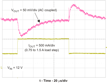
TPS54320 ld_trans_lvs982.gif
Figure 35. Load Transient
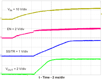
TPS54320 stup_vin_lvs982.gif
Figure 36. Start-Up With VIN (1.1-Ω Load)
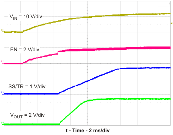
TPS54320 stup2_vin_lvs982.gif
Figure 37. Start-Up With VIN (No Load)
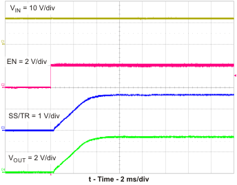
TPS54320 stup4_vin_lvs982.gif
Figure 39. Start-Up With EN (No Load)
TPS54320 vout2_05v_lvs982.gif
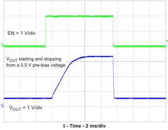
Figure 41. Start-Up and Shutdown With Prebias on EN
(1.1-Ω Load)
TPS54320 vout4_en2_lvs982.gif
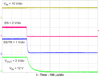
Figure 43. Shutdown With EN (1.1-Ω Load)
TPS54320 vin200_ph_lvs982.gif
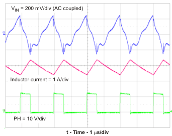
Figure 45. Input Voltage Ripple (1.1-Ω Load)
TPS54320 gain_ph_lvs982.gif
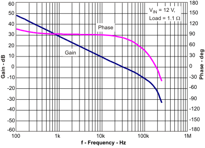
Figure 47. Closed Loop Response
TPS54320 load_reg_lvs982.gif
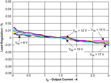
Figure 49. Load Regulation
TPS54320 tc49_lvs982.gif
Figure 51. Maximum Ambient Temperature vs Load Current
TPS54320 tc51_lvs982.gif
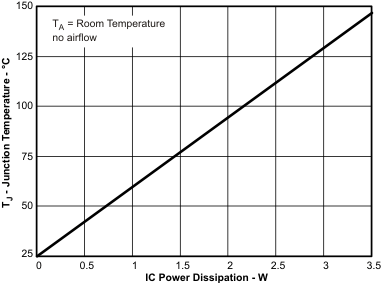
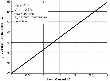
Figure 53. Junction Temperature vs IC Power Dissipation
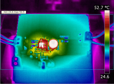
TPS54320 therm_sig_lvs982.gif
VIN = 12 V VOUT = 3.3 V / 3 A
TA = Room temperature
Figure 55. Thermal Signature of TPS54320EVM-513
TPS54320 stup3_vin_lvs982.gif
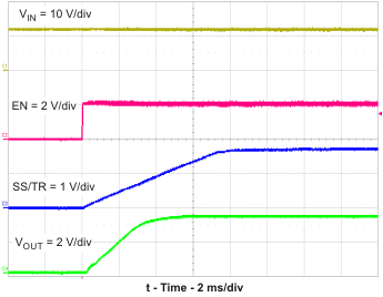
Figure 38. Start-Up With EN (1.1-Ω Load)
TPS54320 vout1_05v_lvs982.gif
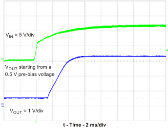
Figure 40. Start-Up With Prebias on VIN (1.1-Ω Load)
TPS54320 vout3_en2_lvs982.gif
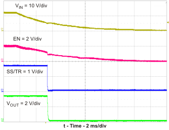
Figure 42. Shutdown With VIN (1.1-Ω Load)
TPS54320 vout1_ph_lvs982.gif
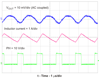
Figure 44. Output Voltage Ripple (1.1-Ω Load)
TPS54320 vo2_ph10_lvs982.gif
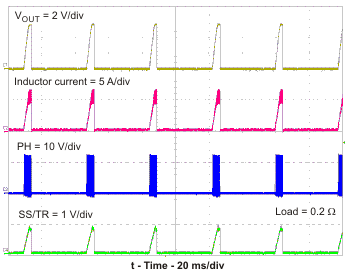
Figure 46. Overcurrent Hiccup Mode
TPS54320 line_reg_lvs982.gif
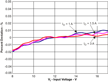
Figure 48. Line Regulation
TPS54320 track_lvs982.gif
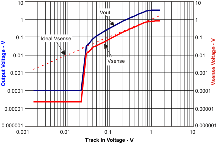
Figure 50. Tracking Performance
TPS54320 tc50_lvs982.gif
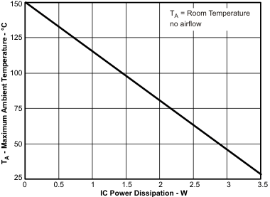
Figure 52. Maximum Ambient Temperature vs IC Power Dissipation
TPS54320 load2_eff_lvs982.gif
Figure 54. Efficiency vs Load Current