ZHCSQS0E August 2006 – January 2024 TPS5410
PRODUCTION DATA
- 1
- 1 特性
- 2 应用
- 3 说明
- 4 Pin Configuration and Functions
- 5 Specifications
-
6 Detailed Description
- 6.1 Overview
- 6.2 Functional Block Diagram
- 6.3
Feature Description
- 6.3.1 Oscillator Frequency
- 6.3.2 Voltage Reference
- 6.3.3 Enable (ENA) and Internal Slow-Start
- 6.3.4 Undervoltage Lockout (UVLO)
- 6.3.5 Boost Capacitor (BOOT)
- 6.3.6 Output Feedback (VSENSE)
- 6.3.7 Internal Compensation
- 6.3.8 Voltage Feed-Forward
- 6.3.9 Pulse-Width-Modulation (PWM) Control
- 6.3.10 Overcurrent Limiting
- 6.3.11 Overvoltage Protection
- 6.3.12 Thermal Shutdown
- 6.4 Device Functional Modes
-
7 Applications and Implementation
- 7.1 Application Information
- 7.2
Typical Applications
- 7.2.1 Application Circuit
- 7.2.2 Using All Ceramic Capacitors
- 7.3 Power Supply Recommendations
- 7.4 Layout
- 8 Device and Documentation Support
- 9 Revision History
- 10Mechanical, Packaging, and Orderable Information
7.2.1.2.3.2 Capacitor Selection
The important design factors for the output capacitor are dc voltage rating, ripple current rating, and equivalent series resistance (ESR). The dc voltage and ripple current ratings cannot be exceeded. The ESR is important because along with the inductor ripple current it determines the amount of output ripple voltage. The actual value of the output capacitor is not critical, but some practical limits do exist. Consider the relationship between the desired closed loop crossover frequency of the design and LC corner frequency of the output filter. Due to the design of the internal compensation, TI recommends to keep the closed loop crossover frequency in the range 3 kHz to 30 kHz as this frequency range has adequate phase boost to allow for stable operation. For this design example, the intended closed loop crossover frequency is between 2590 Hz and 24 kHz, and below the ESR zero of the output capacitor. Under these conditions, the closed loop crossover frequency is related to the LC corner frequency as:
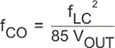
and the desired output capacitor value for the output filter to:

For a desired crossover of 10 kHz and a 68-μH inductor, the calculated value for the output capacitor is 36.5 μF. The capacitor type must be chosen so that the ESR zero is above the loop crossover. The maximum ESR is:
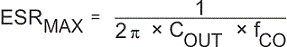
The maximum ESR of the output capacitor also determines the amount of output ripple as specified in the initial design parameters. The output ripple voltage is the inductor ripple current times the ESR of the output filter. Check that the maximum specified ESR as listed in the capacitor data sheet results in an acceptable output ripple voltage:
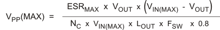
Where:
ΔVPP is the desired peak-to-peak output ripple.
NC is the number of parallel output capacitors.
FSW is the switching frequency.
The minimum ESR of the output capacitor must also be considered. For a good phase margin, if the ESR is zero when the ESR is at its minimum, it must not be above the internal compensation poles at 24 kHz and 54 kHz.
The selected output capacitor must also be rated for a voltage greater than the desired output voltage plus one half the ripple voltage. Any derating amount must also be included. The maximum RMS ripple current in the output capacitor is given by Equation 11:
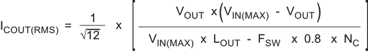
Where:
NC is the number of output capacitors in parallel.
FSW is the switching frequency.
For this design example, a single 47-μF output capacitor is chosen for C3. This value is close to the calculated value of 36.5 μF and yields an actual closed loop cross over frequency of 10.05 kHz. The calculated RMS ripple current is 84.9 mA and the maximum ESR required is 339 mΩ. A capacitor that meets these requirements is a AVX TPSE476M020R0150, rated at 20 V with a maximum ESR of 150 mΩ and a ripple current rating of 1.369 A. This capacitor results in a peak-to-peak output ripple of 44 mV using equation 10. An additional small 0.1-μF ceramic bypass capacitor can also used, but is not included in this design.
Other capacitor types can be used with the TPS5410, depending on the needs of the application.