ZHCSF57 June 2016 TPS51200-EP
PRODUCTION DATA.
- 1 特性
- 2 应用范围
- 3 说明
- 4 修订历史记录
- 5 Pin Configuration and Functions
- 6 Specifications
-
7 Detailed Description
- 7.1 Overview
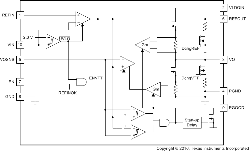
- 7.2 Functional Block Diagram
- 7.3
Feature Description
- 7.3.1 Sink and Source Regulator (VO Pin)
- 7.3.2 Reference Input (REFIN Pin)
- 7.3.3 Reference Output (REFOUT Pin)
- 7.3.4 Soft-Start Sequencing
- 7.3.5 Enable Control (EN Pin)
- 7.3.6 Powergood Function (PGOOD Pin)
- 7.3.7 Current Protection (VO Pin)
- 7.3.8 UVLO Protection (VIN Pin)
- 7.3.9 Thermal Shutdown
- 7.3.10 Tracking Start-up and Shutdown
- 7.4 Device Functional Modes
- 8 Application and Implementation
- 9 Power Supply Recommendations
- 10Layout
- 11器件和文档支持
- 12机械、封装和可订购信息
7 Detailed Description
7.1 Overview
The TPS51200-EP device is a sink and source double data rate (DDR) termination regulator specifically designed for low-input voltage, low-cost, low-noise systems where space is a key consideration.
The device maintains a fast transient response and only requires a minimum output capacitance of 20 μF. The device supports a remote sensing function and all power requirements for DDR, DDR2, DDR3, Low-Power DDR3, and DDR4 VTT bus termination.
7.2 Functional Block Diagram

7.3 Feature Description
7.3.1 Sink and Source Regulator (VO Pin)
The TPS51200-EP is a sink and source tracking termination regulator specifically designed for low-input voltage, low-cost, and low-external component count systems where space is a key application parameter. The device integrates a high-performance, low-dropout (LDO) linear regulator that is capable of both sourcing and sinking current. The LDO regulator employs a fast feedback loop so that small ceramic capacitors can be used to support the fast load transient response. To achieve tight regulation with minimum effect of trace resistance, connect a remote sensing terminal, VOSNS, to the positive terminal of each output capacitor as a separate trace from the high-current path from VO.
7.3.2 Reference Input (REFIN Pin)
The output voltage, VO, is regulated to REFOUT. When REFIN is configured for standard DDR termination applications, REFIN can be set by an external equivalent ratio voltage divider connected to the memory supply bus (VDDQ). The TPS51200-EP device supports REFIN voltages from 0.5 V to 1.8 V, making it versatile and ideal for many types of low-power LDO applications.
7.3.3 Reference Output (REFOUT Pin)
When it is configured for DDR termination applications, REFOUT generates the DDR VTT reference voltage for the memory application. It is capable of supporting both a sourcing and sinking load of 10 mA. REFOUT becomes active when REFIN voltage rises to 0.39 V and VIN is above the UVLO threshold. When REFOUT is less than 0.375 V, it is disabled and subsequently discharges to GND through an internal 10-kΩ MOSFET. REFOUT is independent of the EN pin state.
7.3.4 Soft-Start Sequencing
A current clamp implements the soft-start function of the VO pin. The current clamp allows the output capacitors to be charged with low and constant current, providing a linear ramp-up of the output voltage. When VO is outside of the powergood (PGOOD) window, the current clamp level is one-half of the full overcurrent limit (OCL) level. When VO rises or falls within the PGOOD window, the current clamp level switches to the full OCL level. The soft-start function is completely symmetrical and the overcurrent limit works for both directions. The soft-start function works not only from GND to the REFOUT voltage, but also from VLDOIN to the REFOUT voltage.
7.3.5 Enable Control (EN Pin)
When EN is driven high, the VO regulator begins normal operation. When the device drives EN low, VO discharges to GND through an internal 18-Ω MOSFET. REFOUT remains on when the device drives EN low. Ensure that the EN pin voltage remains lower than or equal to VVIN at all times.
7.3.6 Powergood Function (PGOOD Pin)
The TPS51200-EP device provides an open-drain PGOOD output that goes high when the VO output is within ±20% of REFOUT. PGOOD de-asserts within 10 μs after the output exceeds the size of the PGOOD window. During initial VO start-up, PGOOD asserts high 2 ms (typ) after the VO enters PGOOD window. Because PGOOD is an open-drain output, a pull-up resistor with a value between 1 kΩ and 100 kΩ, placed between PGOOD and a stable active supply voltage rail, is required.
7.3.7 Current Protection (VO Pin)
The LDO has a constant overcurrent limit (OCL). The OCL level reduces by one-half when the output voltage is not within the PGOOD window. This reduction is a non-latch protection.
7.3.8 UVLO Protection (VIN Pin)
For VIN undervoltage lockout (UVLO) protection, the TPS51200-EP monitors VIN voltage. When the VIN voltage is lower than the UVLO threshold voltage, both the VO and REFOUT regulators are powered off. This shutdown is a non-latch protection.
7.3.9 Thermal Shutdown
The TPS51200-EP monitors junction temperature. If the device junction temperature exceeds the threshold value, (typically 150°C), the VO and REFOUT regulators both shut off, discharged by the internal discharge MOSFETs. This shutdown is a non-latch protection.
7.3.10 Tracking Start-up and Shutdown
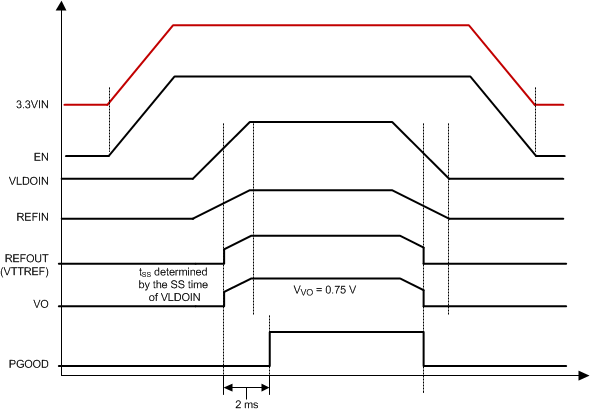
The TPS51200-EP also supports tracking start-up and shutdown when the EN pin is tied directly to the system bus and not used to turn on or turn off the device. During tracking start-up, VO follows REFOUT once REFIN voltage is greater than 0.39 V. REFIN follows the rise of VDDQ rail through a voltage divider. The typical soft-start time (tSS) for the VDDQ rail is approximately 3 ms, however it may vary depending on the system configuration. The soft-start time of the VO output no longer depends on the OCL setting, but it is a function of the soft-start time of the VDDQ rail. PGOOD is asserted 2 ms after VVO is within ±20% of REFOUT. During tracking shutdown, the VO pin voltage falls following REFOUT until REFOUT reaches 0.37 V. When REFOUT falls below 0.37 V, the internal discharge MOSFETs turn on and quickly discharge both REFOUT and VO to GND. PGOOD is deasserted once VO is beyond the ±20% range of REFOUT. Figure 18 shows the typical timing diagram for an application that uses tracking start-up and shutdown.
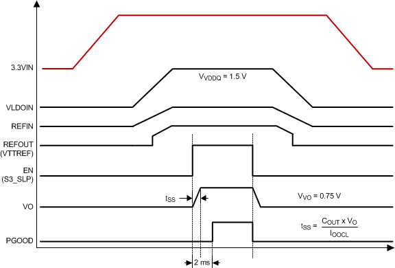
 Figure 17. Typical Timing Diagram for S3 and Pseudo-S5 Support
 Figure 18. Typical Timing Diagram of Tracking Start-up and Shutdown
7.4 Device Functional Modes
7.4.1 Low-Input Voltage Applications
TPS51200-EP can be used in an application system that offers either a 2.5-V rail or a 3.3-V rail. If only a 5-V rail is available, consider using the TPS51100 device as an alternative. The TPS51200-EP device has a minimum input voltage requirement of 2.375 V. If a 2.5-V rail is used, ensure that the absolute minimum voltage (both DC and transient) at the device pin is be 2.375 V or greater. The voltage tolerance for a 2.5-V rail input is between –5% and 5% accuracy, or better.
7.4.2 S3 and Pseudo-S5 Support
The TPS51200-EP provides S3 support by an EN function. The EN pin could be connected to an SLP_S3 signal in the end application. Both REFOUT and VO are on when EN = high (S0 state). REFOUT is maintained while VO is turned off and discharged via an internal discharge MOSFET when EN = low (S3 state). When EN = low and the REFIN voltage is less than 0.39 V, TPS51200-EP enters pseudo-S5 state. Both VO and REFOUT outputs are turned off and discharged to GND through internal MOSFETs when pseudo-S5 support is engaged (S4 or S5 state). Figure 17 shows a typical start-up and shutdown timing diagram for an application that uses S3 and pseudo-S5 support.