ZHCSO14A March   2017  – September 2021 TPS3851-Q1

PRODUCTION DATA  

  1. 特性
  2. 应用
  3. 说明
  4. Revision History
  5. Pin Configuration and Functions
  6. Specifications
    1. 6.1 Absolute Maximum Ratings
    2. 6.2 ESD Ratings
    3. 6.3 Recommended Operating Conditions
    4. 6.4 Thermal Information
    5. 6.5 Electrical Characteristics
    6. 6.6 Timing Requirements
    7. 6.7 Timing Diagrams
    8. 6.8 Typical Characteristics
  7. Detailed Description
    1. 7.1 Overview
    2. 7.2 Functional Block Diagram
    3. 7.3 Feature Description
      1. 7.3.1 RESET
      2. 7.3.2 Manual Reset MR
      3. 7.3.3 UV Fault Detection
      4. 7.3.4 Watchdog Mode
        1. 7.3.4.1 CWD
        2. 7.3.4.2 Watchdog Input WDI
        3. 7.3.4.3 Watchdog Output WDO
        4. 7.3.4.4 SET1
    4. 7.4 Device Functional Modes
      1. 7.4.1 VDD is Below VPOR ( VDD < VPOR)
      2. 7.4.2 Above Power-On-Reset, But Less Than VDD(min) (VPOR ≤ VDD < VDD(min))
      3. 7.4.3 Normal Operation (VDD ≥ VDD(min))
  8. Application and Implementation
    1. 8.1 Application Information
      1. 8.1.1 CWD Functionality
        1. 8.1.1.1 Factory-Programmed Timing Options
        2. 8.1.1.2 Adjustable Capacitor Timing
      2. 8.1.2 Overdrive Voltage
    2. 8.2 Typical Application
      1. 8.2.1 Design Requirements
      2. 8.2.2 Detailed Design Procedure
        1. 8.2.2.1 Monitoring the 1.8-V Rail
        2. 8.2.2.2 Calculating the RESET and WDO Pullup Resistor
        3. 8.2.2.3 Setting the Watchdog
        4. 8.2.2.4 Watchdog Disabled During Initialization Period
      3. 8.2.3 Glitch Immunity
      4. 8.2.4 Application Curves
  9. Power Supply Recommendations
  10. 10Layout
    1. 10.1 Layout Guidelines
    2. 10.2 Layout Example
  11. 11Device and Documentation Support
    1. 11.1 Device Support
      1. 11.1.1 Device Nomenclature
    2. 11.2 Documentation Support
      1. 11.2.1 Related Documentation
    3. 11.3 接收文档更新通知
    4. 11.4 支持资源
    5. 11.5 Trademarks
    6. 11.6 Electrostatic Discharge Caution
    7. 11.7 术语表
  12. 12Mechanical, Packaging, and Orderable Information

封装选项

机械数据 (封装 | 引脚)
散热焊盘机械数据 (封装 | 引脚)
订购信息

Calculating the RESET and WDO Pullup Resistor

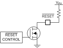
Figure 8-4 shows the TPS3851-Q1 using an open-drain configuration for the RESET circuit. When the FET is off, the resistor pulls the drain of the transistor to VDD and when the FET is turned on, the FET attempts to pull the drain to ground, thus creating an effective resistor divider. The resistors in this divider must be chosen to ensure that VOL is below the maximum value. To choose the proper pullup resistor, there are three key specifications to keep in mind: the pullup voltage (VPU), the recommended maximum RESET pin current (IRESET), and VOL. The maximum VOL is 0.4 V, meaning that the effective resistor divider created must be able to bring the voltage on the reset pin below 0.4 V with IRESET kept below 10 mA. For this example, with a VPU of 1.8 V, a resistor must be chosen to keep IRESET below 50 μA because this value is the maximum consumption current allowed. To ensure this specification is met, a pullup resistor value of 100 kΩ was selected, which sinks a maximum of 18 μA when RESET or WDO is asserted. As illustrated in Figure 6-13, the RESET current is at 18 μA and the low-level output voltage is approximately zero.
GUID-234EA970-8244-426D-BAD5-9B6637EC1E7B-low.gifFigure 8-4 RESET Open-Drain Configuration