ZHCSO14A March   2017  – September 2021 TPS3851-Q1

PRODUCTION DATA  

  1. 特性
  2. 应用
  3. 说明
  4. Revision History
  5. Pin Configuration and Functions
  6. Specifications
    1. 6.1 Absolute Maximum Ratings
    2. 6.2 ESD Ratings
    3. 6.3 Recommended Operating Conditions
    4. 6.4 Thermal Information
    5. 6.5 Electrical Characteristics
    6. 6.6 Timing Requirements
    7. 6.7 Timing Diagrams
    8. 6.8 Typical Characteristics
  7. Detailed Description
    1. 7.1 Overview
    2. 7.2 Functional Block Diagram
    3. 7.3 Feature Description
      1. 7.3.1 RESET
      2. 7.3.2 Manual Reset MR
      3. 7.3.3 UV Fault Detection
      4. 7.3.4 Watchdog Mode
        1. 7.3.4.1 CWD
        2. 7.3.4.2 Watchdog Input WDI
        3. 7.3.4.3 Watchdog Output WDO
        4. 7.3.4.4 SET1
    4. 7.4 Device Functional Modes
      1. 7.4.1 VDD is Below VPOR ( VDD < VPOR)
      2. 7.4.2 Above Power-On-Reset, But Less Than VDD(min) (VPOR ≤ VDD < VDD(min))
      3. 7.4.3 Normal Operation (VDD ≥ VDD(min))
  8. Application and Implementation
    1. 8.1 Application Information
      1. 8.1.1 CWD Functionality
        1. 8.1.1.1 Factory-Programmed Timing Options
        2. 8.1.1.2 Adjustable Capacitor Timing
      2. 8.1.2 Overdrive Voltage
    2. 8.2 Typical Application
      1. 8.2.1 Design Requirements
      2. 8.2.2 Detailed Design Procedure
        1. 8.2.2.1 Monitoring the 1.8-V Rail
        2. 8.2.2.2 Calculating the RESET and WDO Pullup Resistor
        3. 8.2.2.3 Setting the Watchdog
        4. 8.2.2.4 Watchdog Disabled During Initialization Period
      3. 8.2.3 Glitch Immunity
      4. 8.2.4 Application Curves
  9. Power Supply Recommendations
  10. 10Layout
    1. 10.1 Layout Guidelines
    2. 10.2 Layout Example
  11. 11Device and Documentation Support
    1. 11.1 Device Support
      1. 11.1.1 Device Nomenclature
    2. 11.2 Documentation Support
      1. 11.2.1 Related Documentation
    3. 11.3 接收文档更新通知
    4. 11.4 支持资源
    5. 11.5 Trademarks
    6. 11.6 Electrostatic Discharge Caution
    7. 11.7 术语表
  12. 12Mechanical, Packaging, and Orderable Information

封装选项

机械数据 (封装 | 引脚)
散热焊盘机械数据 (封装 | 引脚)
订购信息

UV Fault Detection

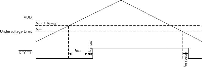
The TPS3851-Q1 features undervoltage detection for common rails between 1.8 V and 5 V. The voltage is monitored on the input rail of the device. If VDD drops below VITN, then RESET is asserted (driven low).
Figure 7-1 shows that when VDD is above VITN + VHYST, RESET deasserts after tRST. The internal comparator has built-in hysteresis that provides some noise immunity and ensures stable operation. Although not required in most cases, for noisy applications, good analog design practice is to place a 1-nF to 100-nF bypass capacitor close to the VDD pin to reduce sensitivity to transient voltages on the monitored signal.
GUID-890AE0EF-4554-4D3F-A731-7543E3747462-low.gifFigure 7-1 Undervoltage Detection