ZHCSS26F november 1998 – october 2020
PRODUCTION DATA
- 1
- 1 特性
- 2 应用
- 3 说明
- 4 Revision History
- 5 Device Comparison Table
- 6 Pin Configuration and Functions
-
7 Specifications
- 7.1 Absolute Maximum Ratings
- 7.2 ESD Ratings
- 7.3 Recommended Operating Conditions
- 7.4 Thermal Information
- 7.5 Electrical Characteristics
- 7.6 Electrical Characteristics for TPS3705-33 Only
- 7.7 Timing Requirements
- 7.8 Switching Characteristics
- 7.9 Dissipation Ratings
- 7.10 Timing Diagram
- 7.11 Typical Characteristics
- 8 Detailed Description
- 9 Application and Implementation
- 10Power Supply Recommendations
- 11Layout
- 12Device and Documentation Support
- 13Mechanical, Packaging, and Orderable Information
封装选项
机械数据 (封装 | 引脚)
散热焊盘机械数据 (封装 | 引脚)
- DGN|8
订购信息
7.11 Typical Characteristics
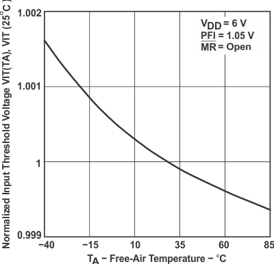 Figure 7-2 Normalized
Input Threshold Voltage vs Free-Air Temperature at VDD
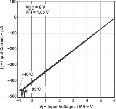 Figure 7-4 Input Current
vs Input Voltage at MR
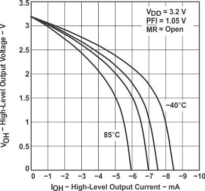 Figure 7-6 High-Level
Output Voltage vs High-Level Output Current
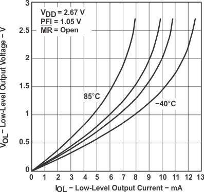 Figure 7-8 Low-Level
Output Voltage vs Low-Level Output Current
 Figure 7-10 Watchdog Timeout Histogram for
TSP3705-33 Devices at 25°C (Unit Count = 20)
 Figure 7-12 Reset Delay Histogram for TPS3705-33
Devices at -40°C (Unit Count = 20)
 Figure 7-14 Reset Delay Histogram for TPS3705-33
Devices at 125°C (Unit Count = 20)
 Figure 7-16 MR to
RESET (tPHL) Delay Histogram for TPS3705-33 Devices at
25°C (Unit Count = 20)
 Figure 7-18 VDD to
RESET (tPHL) Delay Histogram for TPS3705-33 Devices at
-40°C (Unit Count = 20)
 Figure 7-20 VDD to
RESET (tPHL) Delay Histogram for TPS3705-33 Devices at
125°C (Unit Count = 20)
 Figure 7-22 PFI to PFO
(tPHL) Delay Histogram for TPS3705-33 Devices at 25°C (Unit Count =
20)
 Figure 7-24 PFI to PFO
(tPLH) Delay Histogram for TPS3705-33 Devices at -40°C (Unit Count =
20)
 Figure 7-26 PFI to PFO
(tPLH) Delay Histogram for TPS3705-33 Devices at 125°C (Unit Count =
20)
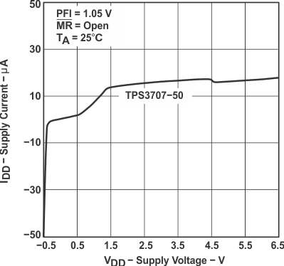 Figure 7-3 Supply Current
vs Supply Voltage
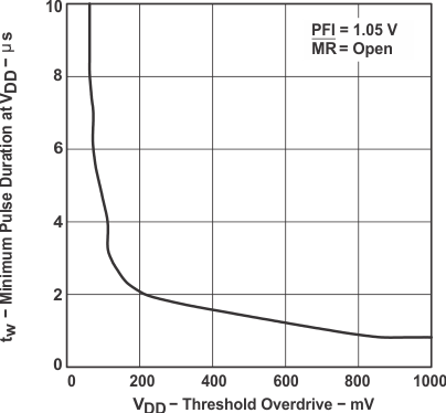 Figure 7-5 Minimum Pulse
Duration at VDD vs VDD Threshold Overdrive
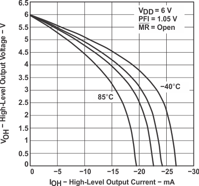 Figure 7-7 High-Level
Output Voltage vs High-Level Output Current
 Figure 7-9 Watchdog Timeout Histogram for
TSP3705-33 Devices at -40°C (Unit Count = 20)
 Figure 7-11 Watchdog Timeout Histogram for
TSP3705-33 Devices at 125°C (Unit Count = 20)
 Figure 7-13 Reset Delay Histogram for TPS3705-33
Devices at 25°C (Unit Count = 20)
 Figure 7-15 MR to
RESET (tPHL) Delay Histogram for TPS3705-33 Devices at
-40°C (Unit Count = 20)
 Figure 7-17 MR to
RESET (tPHL) Delay Histogram for TPS3705-33 Devices at
125°C (Unit Count = 20)
 Figure 7-19 VDD to
RESET (tPHL) Delay Histogram for TPS3705-33 Devices at
25°C (Unit Count = 20)
 Figure 7-21 PFI to PFO
(tPHL) Delay Histogram for TPS3705-33 Devices at -40°C (Unit Count =
20)
 Figure 7-23 PFI to PFO
(tPHL) Delay Histogram for TPS3705-33 Devices at 125°C (Unit Count =
20)
 Figure 7-25 PFI to PFO
(tPLH) Delay Histogram for TPS3705-33 Devices at 25°C (Unit Count =
20)