ZHCSGR0A February 2015 – August 2017 TPS2388
PRODUCTION DATA.
- 1 特性
- 2 应用
- 3 说明
- 4 修订历史记录
- 5 Pin Configuration and Functions
- 6 Specifications
- 7 Parameter Measurement Information
-
8 Detailed Description
- 8.1 Overview
- 8.2 Functional Block Diagram
- 8.3 Feature Description
- 8.4 Device Functional Modes
- 8.5 Programming
- 8.6
Register Maps
- 8.6.1 Complete Register Set
- 8.6.2 INTERRUPT Register
- 8.6.3 INTERRUPT MASK Register
- 8.6.4 POWER EVENT Register
- 8.6.5 DETECTION EVENT Register
- 8.6.6 FAULT EVENT Register
- 8.6.7 START/ILIM EVENT Register
- 8.6.8 SUPPLY EVENT Register
- 8.6.9 PORT 1 STATUS Register
- 8.6.10 PORT 2 STATUS Register
- 8.6.11 PORT 3 STATUS Register
- 8.6.12 PORT 4 STATUS Register
- 8.6.13 POWER STATUS Register
- 8.6.14 Pin Status Register
- 8.6.15 OPERATING MODE Register
- 8.6.16 DISCONNECT ENABLE Register
- 8.6.17 DETECT/CLASS ENABLE Register
- 8.6.18 Port Power Priority/ICUT Disable Register Name
- 8.6.19 TIMING CONFIGURATION Register
- 8.6.20 GENERAL MASK Register
- 8.6.21 DETECT/CLASS RESTART Register
- 8.6.22 POWER ENABLE Register
- 8.6.23 RESET Register
- 8.6.24 ID Register
- 8.6.25 Police 21 Configuration Register
- 8.6.26 Police 43 Configuration Register
- 8.6.27 IEEE Power Enable Register
- 8.6.28 Power-on Fault Register
- 8.6.29 PORT RE-MAPPING Register
- 8.6.30 Port 21 Multi Bit Priority Register
- 8.6.31 Port 43 Multi Bit Priority Register
- 8.6.32 TEMPERATURE Register
- 8.6.33 INPUT VOLTAGE Register
- 8.6.34 PORT 1 CURRENT Register
- 8.6.35 PORT 2 CURRENT Register
- 8.6.36 PORT 3 CURRENT Register
- 8.6.37 PORT 4 CURRENT Register
- 8.6.38 PORT 1 VOLTAGE Register
- 8.6.39 PORT 2 VOLTAGE Register
- 8.6.40 PORT 3 VOLTAGE Register
- 8.6.41 PORT 4 VOLTAGE Register
- 8.6.42 PoE Plus Register
- 8.6.43 FIRMWARE REVISION
- 8.6.44 I2C WATCHDOG Register
- 8.6.45 DEVICE ID Register
- 8.6.46 PORT 1 DETECT RESISTANCE Register
- 8.6.47 PORT 2 DETECT RESISTANCE Register
- 8.6.48 PORT 3 DETECT RESISTANCE Register
- 8.6.49 PORT 4 DETECT RESISTANCE Register
- 9 Application and Implementation
- 10Power Supply Recommendations
- 11Layout
- 12器件和文档支持
- 13机械、封装和可订购信息
6 Specifications
6.1 Absolute Maximum Ratings
over operating free-air temperature range (unless otherwise noted) (1)| MIN | MAX | UNIT | ||
|---|---|---|---|---|
| Input voltage | VPWR | –0.3 | 70 | V |
| VDD | –0.3 | 4 | V | |
| OSS, RESET, A1-A4 | –0.3 | 4 | V | |
| SEN1-8,(6) KSENSA, KSENSB, KSENSC, KSENSD | –0.3 | 3 | V | |
| Output voltage | GATE1-8(2) (4) | –0.3 | 12 | V |
| Voltage | SDAI, SDAO (3) , SCL, INT | –0.3 | 4 | V |
| DRAIN1-8 (3) (5) | –0.3 | 70 | V | |
| TEST0-3, ATST_DCPL0, DTST_DCPL1(3) | –0.3 | 4 | V | |
| AGND | –0.3 | 0.3 | V | |
| Sink current | INT, SDAO | 20 | mA | |
| Lead temperature 1.6 mm (1/16-inch) from case for 10 seconds | 260 | °C | ||
| Tstg | Storage temperature | –65 | 150 | °C |
(1) Stresses beyond those listed under Absolute Maximum Ratings may cause permanent damage to the device. These are stress ratings only, which do not imply functional operation of the device at these or any other conditions beyond those indicated under Recommended Operating Conditions. Exposure to absolute-maximum-rated conditions for extended periods may affect device reliability.
(2) Application of voltage is not implied; these are internally driven pins.
(3) Do not apply external voltage sources directly
(4) If the external MOSFET fails short between its drain and gate, the GATE pin may internally permanently disconnect to prevent cascade damage. The three other ports continue to operate.
(5) Short transients (µs range) up to 80 V are allowed
(6) SEN1-8 are tolerant to 15-V transients to avoid fault propagation when a MOSFET fails in short-circuit
6.2 ESD Ratings
| VALUE | UNIT | |||
|---|---|---|---|---|
| V(ESD) | Electrostatic discharge | Human body model (HBM), per ANSI/ESDA/JEDEC JS-001, all pins(1) | ±2000 | V |
| Charged device model (CDM), per JEDEC specification JESD22-C101, all pins(2) | ±500 | |||
(1) JEDEC document JEP155 states that 500-V HBM allows safe manufacturing with a standard ESD control process.
(2) JEDEC document JEP157 states that 250-V CDM allows safe manufacturing with a standard ESD control process.
6.3 Recommended Operating Conditions
over operating free-air temperature range (unless otherwise noted)| MIN | NOM | MAX | UNIT | ||
|---|---|---|---|---|---|
| VVDD | 3 | 3.3 | 3.6 | V | |
| VVPWR | 44 | 48 | 57 | V | |
| Voltage slew rate on VPWR | 1 | V/µs | |||
| TJ | Operating junction temperature | –40 | 125 | °C | |
| TA | Operating free-air temperature | –40 | 85 | °C |
6.4 Thermal Information
| THERMAL METRIC(1) | TPS2388 | UNIT | |
|---|---|---|---|
| VQFN (56 PINS) | |||
| RθJA | Junction-to-ambient thermal resistance | 25.3 | °C/W |
| RθJC(top) | Junction-to-case (top) thermal resistance | 9.7 | |
| RθJB | Junction-to-board thermal resistance | 3.7 | |
| ψJT | Junction-to-top characterization parameter | 0.2 | |
| ψJB | Junction-to-board characterization parameter | 3.7 | |
| RθJC(bot) | Junction-to-case (bottom) thermal resistance | 0.5 | |
(1) For more information about traditional and new thermal metrics, see the IC Package Thermal Metrics application report, SPRA953.
6.5 Electrical Characteristics
–40°C ≤ TJ ≤ 125°C unless otherwise noted. VVDD = 3.3 V, VVPWR = 48 V, VDGND = VAGND, DGND, KSENSA, KSENSB, KSENSC, and KSENSD connected to AGND, and all outputs are unloaded, unless otherwise noted. PoEPn = 0. Positive currents are into pins. RS = 0.255 Ω, to KSENSA (SEN1 or SEN2), to KSENSB (SEN3 or SEN4), to KSENSC (SEN5 or SEN6) or to KSENSD (SEN7 or SEN8). Typical values are at 25°C. All voltages are with respect to AGND, unless otherwise noted. Operating registers loaded with default values, unless otherwise noted.| PARAMETER | TEST CONDITIONS | MIN | TYP | MAX | UNIT | |
|---|---|---|---|---|---|---|
| INPUT SUPPLY VPWR | ||||||
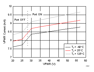
| IVPWR | VPWR current consumption | VVPWR = 50 V | 10 | 12.5 | mA | |
| VVPWR < 8 V | 100 | µA | ||||
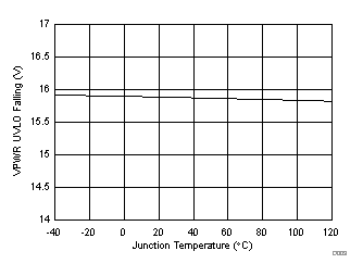
| VUVLOPW_F | VPWR UVLO falling threshold | 14.5 | 17.5 | V | ||
| VUVLOPW_R | VPWR UVLO rising threshold | 15.5 | 18.5 | V | ||
| VPUV_F | VPWR undervoltage falling threshold | VPUV threshold | 25 | 26.5 | 28 | V |
| TOTAL DEVICE POWER DISSIPATION | ||||||
| PT | VPWR and VDD consumption | VVPWR = 50 V | 0.67 | W | ||
| INPUT SUPPLY VDD | ||||||
| IVDD | VDD Current consumption | 6 | 12 | mA | ||
| VUVDD_F | VDD UVLO falling threshold | For port deassertion | 2.1 | 2.25 | 2.4 | V |
| VUVDD_R | VDD UVLO rising threshold | 2.45 | 2.6 | 2.75 | V | |
| VUVDD_HYS | Hysteresis VDD UVLO | 0.35 | V | |||
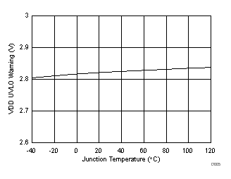
| VUVW_F | VDD UVLO warning threshold | 2.6 | 2.8 | 3.0 | V | |
| DETECTION | ||||||
| IDISC | Detection current | First detection point, VVPWR – VDRAINn = 0 V | 145 | 160 | 190 | µA |
| Second detection point, VVPWR – VDRAINn = 0 V | 235 | 270 | 300 | |||
| High-current detection point, VVPWR – VDRAINn = 0 V | 490 | 540 | 585 | |||
| Vdetect | Open-circuit detection voltage | VVPWR – VDRAINn | 23.5 | 26 | 29 | V |
| RREJ_LOW | Rejected resistance low range | 0.86 | 15 | kΩ | ||
| RREJ_HI | Rejected resistance high range | 33 | 100 | kΩ | ||
| RACCEPT | Accepted resistance range | 19 | 25 | 26.5 | kΩ | |
| RSHORT | Shorted port threshold | 360 | Ω | |||
| ROPEN | Open port threshold | 400 | kΩ | |||
| CLASSIFICATION | ||||||
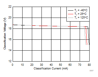
| VCLASS | Classification voltage | VVPWR – VDRAINn, VSENn ≥ 0 mV, Iport ≥ 180 µA |
15.5 | 18.5 | 20.5 | V |
| ICLASS_Lim | Classification current limit | VVPWR – VDRAINn = 0 V | 65 | 75 | 90 | mA |
| ICLASS_TH | Classification threshold current | Class 0-1 | 5 | 8 | mA | |
| Class 1-2 | 13 | 16 | mA | |||
| Class 2-3 | 21 | 25 | mA | |||
| Class 3-4 | 31 | 35 | mA | |||
| Class 4-Class overcurrent | 45 | 51 | mA | |||
| VMARK | Mark voltage | 4 mA ≥ Iport ≥ 180 µA, VVPWR – VDRAINn | 7 | 10 | V | |
| IMARK_Lim | Mark sinking current limit | VVPWR – VDRAINn = 0 V | 10 | 70 | 90 | mA |
| GATE | ||||||
| VGOH | Gate drive voltage | VGATEn , IGATE = –1 µA | 10 | 12.5 | V | |
| IGO- | Gate sinking current with Power-on Reset, OSS detected or port turn off command | VGATEn = 5 V | 60 | 100 | 190 | mA |
| IGO short– | Gate sinking current with port short-circuit | VGATEn = 5 V, VSENn ≥ Vshort (or Vshort2X if 2X mode) | 60 | 100 | 190 | mA |
| IGO+ | Gate sourcing current | VGATEn = 0V | 39 | 50 | 63 | µA |
| DRAIN INPUT | ||||||
| VPGT | Power Good threshold | Measured at VDRAINn | 1.0 | 2.13 | 3 | V |
| VSHT | Shorted FET threshold | Measured at VDRAINn | 4 | 6 | 8 | V |
| RDRAIN | Resistance from DRAINn to VPWR | Any operating mode except during detection or while the port is ON, including in device RESET state | 80 | 100 | 190 | kΩ |
| IDRAIN | DRAINn pin bias current | VVPWR – VDRAINn = 30 V, port ON | 75 | 120 | µA | |
| A/D CONVERTER | ||||||
| tCONV | Conversion time, current measurement | All ranges, each port | 0.64 | 0.8 | 0.96 | ms |
| tCONV_V | Conversion time, voltage measurement | All ranges, each port | 0.82 | 1.03 | 1.2 | ms |
| tGAP | Gap between adjacent current measurement integrations | 5% × tCONV | ms | |||
| Gap between adjacent current averaged results | 5% × tINT_CUR | ms | ||||
| ADCBW | ADC integration bandwidth (–3 db) | Current measurement | 320 | Hz | ||
| tINT_CUR | Integration (averaging) time, current | Each port, port ON current | 82 | 102 | 122 | ms |
| tINT_DET | Integration (averaging) time, detection | 13.1 | 16.6 | 20 | ms | |
| tINT_portV | Integration (averaging) time, port voltage | Port powered | 3.25 | 4.12 | 4.9 | ms |
| tINT_inV | Integration (averaging) time, input voltage | 3.25 | 4.12 | 4.9 | ms | |
| Powered port voltage conversion scale factor and accuracy | At VVPWR – VDRAINn = 57 V | 15097 | 15565 | 16032 | Counts | |
| At VVPWR – VDRAINn = 44 V | 11654 | 12015 | 12375 | Counts | ||
| Powered port current conversion scale factor and accuracy | At port current = 770 mA | 12363 | 12616 | 12868 | Counts | |
| At port current = 7.5 mA | 100 | 123 | 150 | Counts | ||
| Input voltage conversion scale factor and accuracy | At VVPWR = 57 V | 15175 | 15565 | 15955 | Counts | |
| At VVPWR = 44 V | 11713 | 12015 | 12316 | Counts | ||
| δV/Vport | Voltage reading accuracy | At 44 to 57 V | –3% | 3% | ||
| σV | Voltage reading repeatability | Full scale reading | –18 | 18 | mV | |
| δI/Iport | Current reading accuracy | At 50 mA | –3% | 3% | ||
| At 770 mA | -2% | 2% | ||||
| σI | Current reading repeatability | Full scale reading | –7.5 | 7.5 | mA | |
| δR/Rport | Resistance reading accuracy | 15 kΩ ≤ Rport ≤ 33 kΩ, Cport ≤ 0.25 µF, at 44 to 57 V | –7% | 7% | ||
| PORT CURRENT SENSE | ||||||
| VCUT | ICUT limit | VDRAINn = 0 V, POL(3:0) = 0001b | 9.6 | 10.2 | 10.8 | mV |
| VDRAINn = 0 V, POL(3:0) = 0010b | 14.53 | 15.3 | 16.06 | |||
| VDRAINn = 0 V, POL(3:0) = 0111b | 38.76 | 40.8 | 42.84 | |||
| VDRAINn = 0 V, POL(3:0) = 1111b | 77.5 | 81.6 | 85.6 | |||
| VDRAINn = 0 V, POL(3:0) = 0000b, PoEPn = 1 |
77.5 | 81.6 | 85.6 | |||
| VDRAINn = 0 V, POL(3:0) = 1111b, PoEPn = 1 |
222.8 | 234.6 | 246.3 | |||
| δV/Vpolice | Police setting resolution | –6.3% | 6.3% | |||
| δicut/ICUT | ICUT tolerance | All settings except POL(3:0) = 0000b and 0001b while PoEPn = 0 |
–5% | 5% | ||
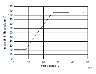
| VInrush | IInrush limit, 1x or 2x mode | VVPWR – VDRAINn = 1 V | 10 | 23 | 31 | mV |
| VVPWR – VDRAINn = 10 V | 20 | 33 | 46 | |||
| VVPWR – VDRAINn = 30 V | 102 | 114.7 | ||||
| VVPWR – VDRAINn = 55 V | 102 | 114.7 | ||||
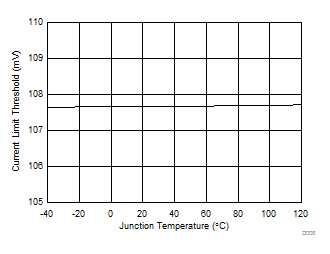
| VLIM | ILIM limit in 1x mode | VDRAINn = 1 V | 102 | 114.7 | mV | |
| VDRAINn = 13 V | 102 | 114.7 | ||||
| VDRAINn = 30 V | 15 | 23 | 31 | |||
| VDRAINn = 48 V | 15 | 23 | 31 | |||
| VLIM2X | ILIM limit in 2X mode (PoEPn = 1) | VDRAINn = 1 V | 260 | 270.3 | 285 | mV |
| VDRAINn = 10 V | 127 | 140 | 153 | |||
| VDRAINn = 30 V | 15 | 23 | 31 | |||
| VDRAINn = 48 V | 15 | 23 | 31 | |||
| Vshort | Ishort threshold in 1X mode and during inrush | Threshold for GATE to be less than 1 V, 2 µS after application of pulse |
234 | 306 | mV | |
| Vshort2X | Ishort threshold in 2X mode | 357 | 408 | |||
| Ibias | Sense pin bias current | Port ON or during class | –2.5 | 0 | µA | |
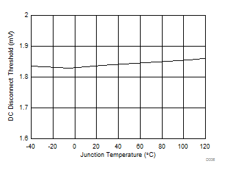
| VIMIN | DC disconnect threshold | 1.275 | 2.55 | mV | ||
| DIGITAL INTERFACE AT VVDD = 3.3 V | ||||||
| VIH | Digital input high | 2.1 | V | |||
| VIL | Digital input low | 0.9 | V | |||
| VIT_HYS | Input voltage hysteresis (SCL, SDAI, A1-A4, RESET, OSS) | 0.17 | V | |||
| VOL | Digital output Low, SDAO | At 9 mA | 0.4 | V | ||
| Digital output Low, INT | At 3 mA | 0.4 | V | |||
| Rpullup | Pullup resistor to VDD | RESET, A1-A4, TEST0 | 30 | 50 | 80 | kΩ |
| Rpulldown | Pulldown resistor to DGND | OSS | 30 | 50 | 80 | kΩ |
| TEST1, 2 | 30 | 50 | 80 | |||
| THERMAL SHUTDOWN | ||||||
| TSD | Shutdown temperature | Temperature rising | 135 | 146 | °C | |
| Hysteresis | 7 | °C | ||||
6.6 Timing Requirements
| MIN | TYP | MAX | UNIT | |||
|---|---|---|---|---|---|---|
| fSCL | SCL clock frequency | 10 | 400 | kHz | ||
| tLOW | LOW period of the clock | 1.3 | µs | |||
| tHIGH | HIGH period of the clock | 0.6 | µs | |||
| tfo | SDAO output fall time | SDAO, 2.3 → 0.8 V, Cb = 10 pF, 10 kΩ pull-up to 3.3 V |
21 | 250 | ns | |
| SDAO, 2.3 → 0.8 V, Cb = 400 pF, 1.3 kΩ pull-up to 3.3 V |
21 | 250 | ns | |||
| CI2C | SCL capacitance | 10 | pF | |||
| CI2C_SDA | SDAI, SDAO capacitance (each) | 6 | pF | |||
| tSU,DATW | Data set-up time (Write operation) | 100 | ns | |||
| tSU,DATR | Data set-up time (Read operation) | SDAO, Cb = 10 pF, 1.3 kΩ pull-up to 3.3V |
600 | ns | ||
| tHD,DATW | Data hold time (Write operation) | 0 | ns | |||
| tHD,DATR | Data hold time (Read operation) | 150 | 600 | ns | ||
| tfSDA | Input fall times of SDAI | 2.3 → 0.8 V | 20 | 250 | ns | |
| trSDA | Input rise times of SDAI | 0.8 → 2.3 V | 20 | 300 | ns | |
| tr | Input rise time of SCL | 0.8 → 2.3 V | 20 | 300 | ns | |
| tf | Input fall time of SCL | 2.3 → 0.8 V | 20 | 200 | ns | |
| tBUF | Bus free time between a STOP and START condition | 1.3 | µs | |||
| tHD,STA | Hold time after (repeated) Start condition | 0.6 | µs | |||
| tSU,STA | Repeated Start condition set-up time | 0.6 | µs | |||
| tSU,STO | Stop condition set-up time | 0.6 | µs | |||
| tFLT_INT | Fault to INT assertion | Time to internally register an Interrupt fault, from port turn off | 50 | 500 | µs | |
| tDG | Suppressed spike pulse width, SDAI and SCL | 50 | ns | |||
| tRDG | RESET input minimum pulse width (deglitch time) | 5 | µs | |||
| tbit_OSS | 3-bit OSS bit period | MbitPrty = 1 | 24 | 25 | 26 | µs |
| tOSS_IDL | Idle time between consecutive shutdown code transmission in 3-bit mode | MbitPrty = 1 | 48 | 50 | µs | |
| tr_OSS | Input rise time of OSS in 3-bit mode | 0.8 → 2.3 V, MbitPrty = 1 | 1 | 300 | ns | |
| tf_OSS | Input fall time of OSS in 3-bit mode | 2.3 → 0.8 V, MbitPrty = 1 | 1 | 300 | ns | |
| tWDT_I2C | I2C Watchdog trip delay | 1.1 | 2.2 | 3.3 | s | |
6.7 Switching Characteristics
over operating free-air temperature range (unless otherwise noted)| PARAMETER | TEST CONDITIONS | MIN | TYP | MAX | UNIT | |
|---|---|---|---|---|---|---|
| δIfault | Duty cycle of Iport with current fault | 5.5% | 6.7% | |||
| tOVLD | ICUT time limit (DCUTn = 0) | TOVLD = 00 | 50 | 70 | ms | |
| TOVLD = 01 | 25 | 35 | ||||
| TOVLD = 10 | 100 | 140 | ||||
| TOVLD = 11 | 200 | 280 | ||||
| tICUT_INT | ICUT Interrupt time limit when ICUT is disabled (DCUTn = 1)(1) | ICUT limit exceeded but not ILIM, TLIM = 01, PoEPn = 1 | tLIM/2 | tLIM/2 + 6 | ms | |
| tLIM | ILIM time limit | 50 | 70 | ms | ||
| TLIM = 00, PoEPn = 1 | 50 | 70 | ||||
| TLIM = 01, PoEPn = 1 | 14.5 | 15 | 15.75 | |||
| TLIM = 10, PoEPn = 1 | 11.5 | 12 | 12.5 | |||
| TLIM = 11, PoEPn = 1 | 9.5 | 10 | 10.5 | |||
| tSTART | Maximum current limit duration in port start-up | TSTART = 00 | 50 | 70 | ms | |
| TSTART = 01 | 25 | 35 | ||||
| TSTART = 10 | 100 | 140 | ||||
| tDET | Detection duration, 4-point discovery | Time to complete a detection | 275 | 350 | 425 | ms |
| tDET_BOFF | Detect backoff pause between discovery attempts | VVPWR – VDRAINn > 2.5 V | 300 | 400 | 500 | ms |
| VVPWR – VDRAINn < 2.5 V | 15 | 100 | ||||
| tDET_DLY | Detection delay | From command or PD attachment to port detection complete | 590 | ms | ||
| tCLE | Classification duration, first and second class event | Semiauto mode. From detection complete | 6.5 | 12 | ms | |
| tpdc | Classification duration, 1-event physical layer class timing | Semiauto mode. From detection complete | 6.5 | 12 | ms | |
| Manual mode. From beginning of class | 6.5 | 14 | ||||
| tME | Mark Duration, first and second mark event | Semiauto mode. From Class 4 complete | 6 | 12 | ms | |
| tpon | Port Power-On delay, semiauto mode | From end of detection to port turn on using IEEE power enable | 200 | ms | ||
| Port Power-On delay, manual mode | From port turn on command to port turn on completed, four ports | 4 | ms | |||
| tRESET | Reset time duration from RESET pin | 1 | 5 | µs | ||
| ted | Error delay timing. Delay before next attempt to power a port following power removal due to error condition | ICUT , ILIM or IInrush fault, semiauto mode | 0.8 | 1 | 1.2 | s |
| tMPDO | PD maintain power signature dropout time limit | TMPDO = 00 | 300 | 400 | ms | |
| TMPDO = 01 | 75 | 100 | ||||
| TMPDO = 10 | 150 | 200 | ||||
| TMPDO = 11 | 600 | 800 | ||||
| tMPS | PD maintain power signature time for validity | 13 | 15 | 17 | ms | |
| tD_off_OSS | Gate turn off time from 1-bit OSS input | From OSS to VGATEn < 1 V, VSENn = 0 V, MbitPrty = 0 | 1 | 5 | µs | |
| tOSS_OFF | Gate turn off time from 3-bit OSS input | From Start bit falling edge to VGATEn < 1 V, VSENn = 0 V, MbitPrty = 1 | 72 | 104 | µs | |
| tP_off_CMD | Gate turn off time from port off command | From port off command to VGATEn < 1 V, VSENn = 0 V | 300 | µs | ||
| tP_off_RST | Gate turn off time with RESET | From RESET low to VGATEn < 1 V, VSENn = 0 V | 1 | 5 | µs | |
| tD_off_SEN | Gate turn off time from SENn input | VDRAINn = 1 V , From VSENn pulsed to 0.425 V | 0.9 | µs | ||
| Gate turn off time from SENn input (PoEPn = 1) | VDRAINn = 1 V , From VSENn pulsed to 0.62 V | 0.9 | ||||
| tPOR | Device power-on reset delay | 20 | ms | |||
(1) The tICUT_INT maximum value shown in the table only applies to a low percentage (< 10%) of occurence. The rest of the time, it becomes tLIM/2 + 2 ms.
6.8 Typical Characteristics
