ZHCSGR0A February 2015 – August 2017 TPS2388
PRODUCTION DATA.
- 1 特性
- 2 应用
- 3 说明
- 4 修订历史记录
- 5 Pin Configuration and Functions
- 6 Specifications
- 7 Parameter Measurement Information
-
8 Detailed Description
- 8.1 Overview
- 8.2 Functional Block Diagram
- 8.3 Feature Description
- 8.4 Device Functional Modes
- 8.5 Programming
- 8.6
Register Maps
- 8.6.1 Complete Register Set
- 8.6.2 INTERRUPT Register
- 8.6.3 INTERRUPT MASK Register
- 8.6.4 POWER EVENT Register
- 8.6.5 DETECTION EVENT Register
- 8.6.6 FAULT EVENT Register
- 8.6.7 START/ILIM EVENT Register
- 8.6.8 SUPPLY EVENT Register
- 8.6.9 PORT 1 STATUS Register
- 8.6.10 PORT 2 STATUS Register
- 8.6.11 PORT 3 STATUS Register
- 8.6.12 PORT 4 STATUS Register
- 8.6.13 POWER STATUS Register
- 8.6.14 Pin Status Register
- 8.6.15 OPERATING MODE Register
- 8.6.16 DISCONNECT ENABLE Register
- 8.6.17 DETECT/CLASS ENABLE Register
- 8.6.18 Port Power Priority/ICUT Disable Register Name
- 8.6.19 TIMING CONFIGURATION Register
- 8.6.20 GENERAL MASK Register
- 8.6.21 DETECT/CLASS RESTART Register
- 8.6.22 POWER ENABLE Register
- 8.6.23 RESET Register
- 8.6.24 ID Register
- 8.6.25 Police 21 Configuration Register
- 8.6.26 Police 43 Configuration Register
- 8.6.27 IEEE Power Enable Register
- 8.6.28 Power-on Fault Register
- 8.6.29 PORT RE-MAPPING Register
- 8.6.30 Port 21 Multi Bit Priority Register
- 8.6.31 Port 43 Multi Bit Priority Register
- 8.6.32 TEMPERATURE Register
- 8.6.33 INPUT VOLTAGE Register
- 8.6.34 PORT 1 CURRENT Register
- 8.6.35 PORT 2 CURRENT Register
- 8.6.36 PORT 3 CURRENT Register
- 8.6.37 PORT 4 CURRENT Register
- 8.6.38 PORT 1 VOLTAGE Register
- 8.6.39 PORT 2 VOLTAGE Register
- 8.6.40 PORT 3 VOLTAGE Register
- 8.6.41 PORT 4 VOLTAGE Register
- 8.6.42 PoE Plus Register
- 8.6.43 FIRMWARE REVISION
- 8.6.44 I2C WATCHDOG Register
- 8.6.45 DEVICE ID Register
- 8.6.46 PORT 1 DETECT RESISTANCE Register
- 8.6.47 PORT 2 DETECT RESISTANCE Register
- 8.6.48 PORT 3 DETECT RESISTANCE Register
- 8.6.49 PORT 4 DETECT RESISTANCE Register
- 9 Application and Implementation
- 10Power Supply Recommendations
- 11Layout
- 12器件和文档支持
- 13机械、封装和可订购信息
9 Application and Implementation
NOTE
Information in the following applications sections is not part of the TI component specification, and TI does not warrant its accuracy or completeness. TI’s customers are responsible for determining suitability of components for their purposes. Customers should validate and test their design implementation to confirm system functionality.
9.1 Application Information
9.1.1 Introduction to PoE
Power-over-Ethernet (PoE) is a means of distributing power to Ethernet devices over the Ethernet cable using either data or spare pairs. PoE eliminates the need for power supplies at the Ethernet device. Common applications of PoE are security cameras, IP Phones and PDA chargers. The host or mid-span equipment that supplies power is the power source equipment (PSE). The load at the Ethernet connector is the powered device (PD). PoE protocol between PSE and PD controlling power to the load is specified by IEEE Std 802.3at-2009. Transformers are used at Ethernet host ports, mid-spans and hubs, to interface data to the cable. A DC voltage can be applied to the center tap of the transformer with no effect on the data signals. As in any power transmission line, a relatively high 48 V is used to keep current low, minimize the effect of IR drops in the line and preserve power to the load. Standard POE delivers approximately 13 W to a type 1 PD, and 25.5 W to a type 2 PD.
9.1.2 TPS2388 Application
The TPS2388 is an 8-port, IEEE 802.3at PoE PSE controller and can be used in high port count semiauto or fully micro-controller managed applications (The MSP430G2553 micro-controller is recommended for most applications). Subsequent sections describe detailed design procedures for applications with different requirements including host control.
The schematic of Figure 71 depicts semiauto mode operation of the TPS2388, providing functionality to power PoE loads. In Figure 71 the TPS2388 can do the following:
- Performs load detection.
- Performs classification including type-2 (two-finger) of up to Class 4 loads.
- Enables power with protective foldback current limiting, and POLICE (ICUT) value.
- Shuts down in the event of fault loads and shorts.
- Performs Maintain Power Signature function to insure removal of power if load is disconnected.
- Undervoltage lock out occurs if VPWR falls below VPUV_F (typical 26.5 V).
Following a power-off command, disconnect or shutdown due to a start, ICUT or ILIM fault, the port powers down. Following port power off due to a power off command or disconnect, the TPS2388 will restart a detection cycle if commanded to do so through I2C bus. If the shutdown is due to a start, ICUT or ILIM fault, the TPS2388 enters into a cool-down period during which any Detect/Class Enable Command for that port will be delayed. At the end of cool down cycle, one or more detection/class cycles are automatically restarted if the class and/or detect enable bits are set.
9.1.3 Kelvin Current Sensing Resistor
Load current in each PSE port is sensed as the voltage across a low-end current-sense resistor with a value of 255 mΩ. For more accurate current sensing, kelvin sensing of the low end of the current-sense resistor is provided through pins KSENSA for ports 1 and 2, KSENSB for ports 3 and 4, KSENSC for ports 5 and 6 and KSENSD for ports 7 and 8.
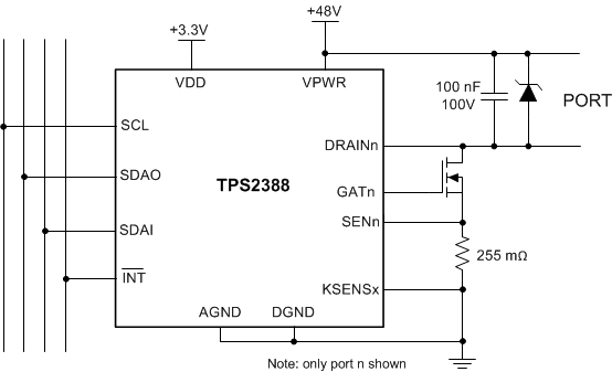 Figure 69. Kelvin Current-Sense Connection
9.1.4 Connections on Unused Ports
On unused ports, it is recommended to ground the SENx pin and leave the GATx pin open. DRAINx pins can be grounded or left open (leaving open may slightly reduce power consumption). Figure 70 shows an example of an unused PORT4.
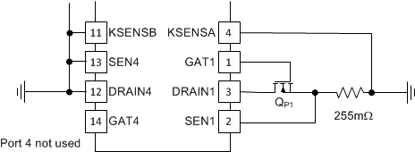 Figure 70. Unused PORT4 Connections
9.2 Typical Application
This typical application shows an eight port, semiauto mode application using MSP430 microcontroller. Operation in any mode requires I2C host support. The TPS2388 provides useful telemetry in multi-port applications to aid in implementing port power management.
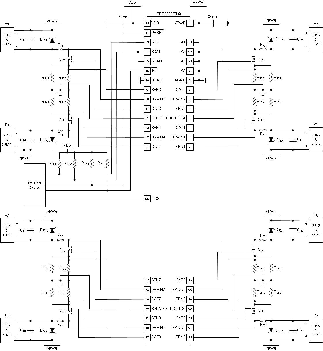 Figure 71. Eight Port Semiauto Mode Application
9.2.1 Design Requirements
The RESET pin may be connected to the micro-controller if an external RESET is required or connected directly to VDD. TPS2388 devices are used in the eight port configuration and are managed by the I2C host device. The I2C address for TPS2388 is programmed using the A4..A1 pins.
9.2.2 Detailed Design Procedure
9.2.2.1 Power Pin Bypass Capacitors
- CVPWR: 0.1 μF, 100 V, X7R ceramic at pin 17 (VPWR)
- CVDD: 0.1 μF, 50 V, X7R ceramic at pin 43 (VDD)
9.2.2.2 Per Port Components
- CPn: 0.1-μF, 100-V, X7R ceramic between VPWR and Pn-
- RSnA / RSnB: The port current sense resistors are a combination of two 0.51-Ω, 1% resistors in parallel (0.255 Ω). Dual 0.51-Ω, 1%, 0.25-W resistors in an 0805 SMT package are recommended. If a nominal 640 mA Policing (ICUT) threshold is selected, the maximum power dissipation for the resistor pair becomes approximately 115 mW (~57 mW each).
- QPn: The port MOSFET can be a small, inexpensive device with average performance characteristics. BVDSS should be 100 V minimum. Target a MOSFET RDS(on) at VGS = 10 V of between 50 mΩ and 150 mΩ. The MOSFET GATE charge (QG) and input capacitance (CISS) should be less than 50 nC and 2000 pF respectively. The maximum power dissipation for QPn with RDS(on) = 100 mΩ at 640 mA nominal policing (ICUT) threshold is approximately 45 mW.
- FPn: The port fuse should be a slow blow type rated for at least 60 VDC and above ~2 x ICUT(max). The cold resistance should be below 200 mΩ to reduce the DC losses. The power dissipation for FPn with a cold resistance of 180 mΩ at maximum ICUT is approximately 81 mW.
- DPnA: The port TVS should be rated for the expected port surge environment. DPnA should have a minimum reverse standoff voltage of 58 V, peak pulse power rating of 600 W, and a maximum clamping voltage of less than 95 V at the expected peak surge current
9.2.2.3 System Level Components (not shown in the schematic diagrams)
The system TVS and bulk VPWR capacitance work together to protect the PSE system from surge events which could cause VPWR to surge above 70 V. The TVS and bulk capacitors should be placed on the PCB such that all TPS2388 ports are adequately protected.
- TVS: The system TVS should have a minimum reverse standoff voltage of 58 V and a peak pulse power rating of 600 W or 1500 W depending on the total number of system ports and amount of bulk VPWR capacitance used. Together with the VPWR bulk capacitance, the TVS must prevent the VPWR rail from exceeding 70 V.
- Bulk Capacitor: The system bulk capacitor(s) should be rated for 100 V and can be of aluminum electrolytic type. Two 47-μF capacitors can be used for each TPS2388 on board.
- Distributed Capacitance:In higher port count systems, it may be necessary to distribute 1-uF, 100-V, X7R ceramic capacitors across the 48-V power bus. One capacitor per each TPS2388 pair is recommended.
- Digital I/O Pullup Resistors: RESET and A1-A4 are internally pulled up to VDD, while OSS is internally pulled down, each with a 50-kΩ (typical) resistor. A stronger pull-up/down resistor can be added externally such as a 10 kΩ, 1%, 0.063 W type in a SMT package. SCL, SDAI, SDAO, and INT require external pull-up resistors within a range of 1 kΩ to 10 kΩ depending on the total number of devices on the bus .
- Ethernet Data Transformer (per port): The Ethernet data transformer must be rated to operate within the IEEE802.3at standard in the presence of the DC port current conditions. The transformer is also chosen to be compatible with the Ethernet PHY. The transformer may also be integrated into the RJ45 connector and cable terminations.
- RJ45 Connector (per port): The majority of the RJ45 connector requirements are mechanical in nature and include tab orientation, housing type (shielded or unshielded), or highly integrated. An integrated RJ45 consists of the Ethernet data transformer and cable terminations at a minimum. The integrated type may also contain the port TVS and common mode EMI filtering.
- Cable Terminations (per port): The cable terminations typically consist of series resistor (usually 75 Ω) and capacitor (usually 10 nF) circuits from each data transformer center tap to a common node which is then bypassed to a chassis ground (or system earth ground) with a high-voltage capacitor (usually 1000 pF to 4700 pF at 2 kV).
9.2.3 Application Curves
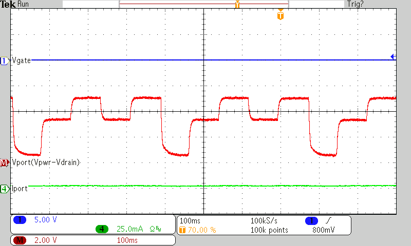
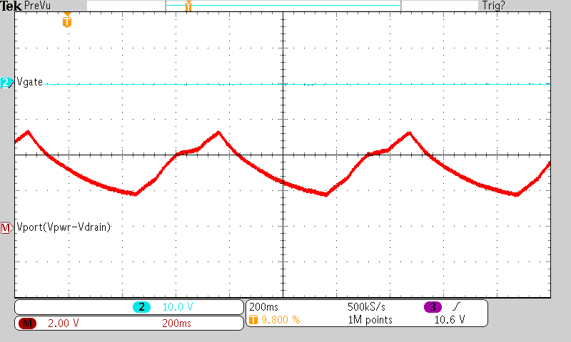
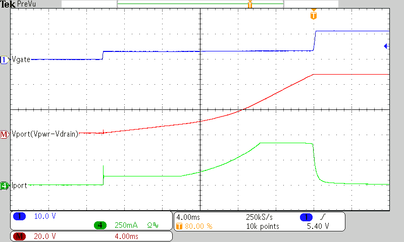
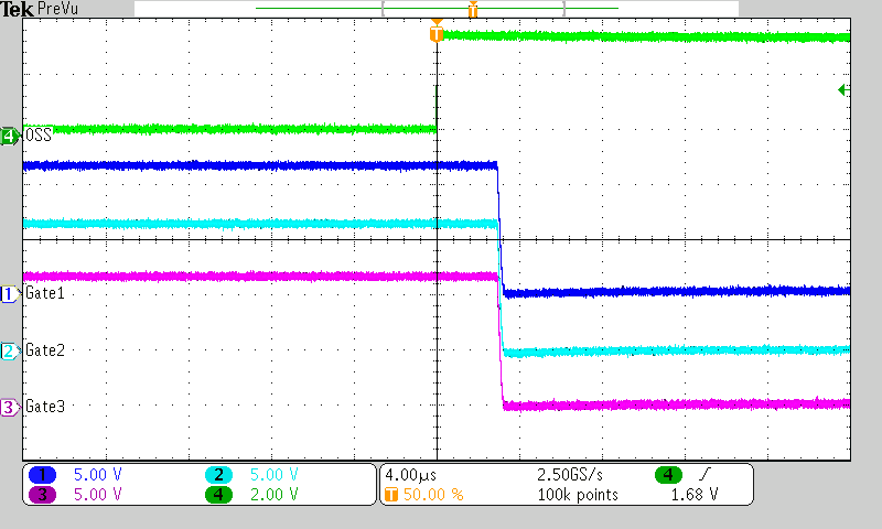
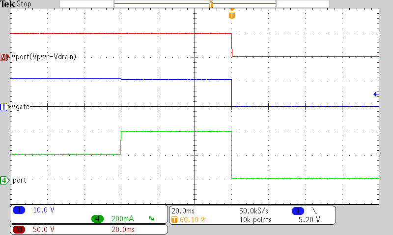
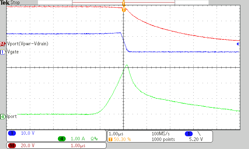
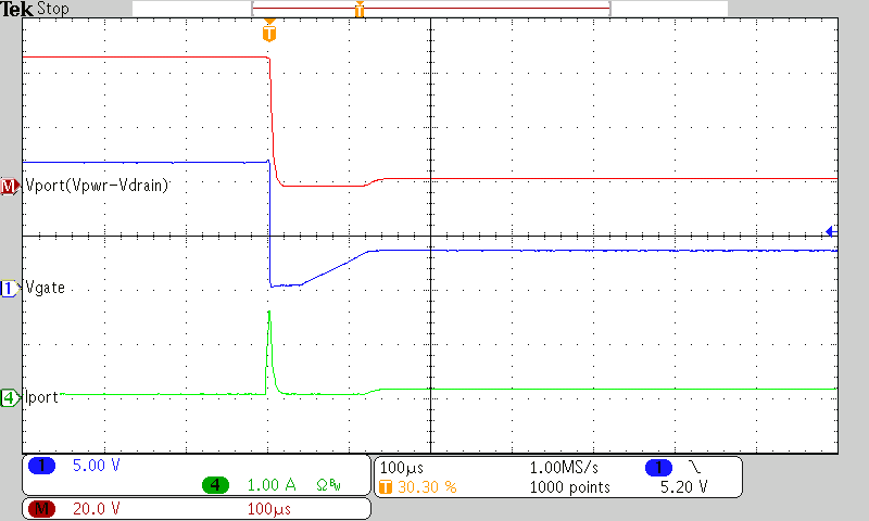
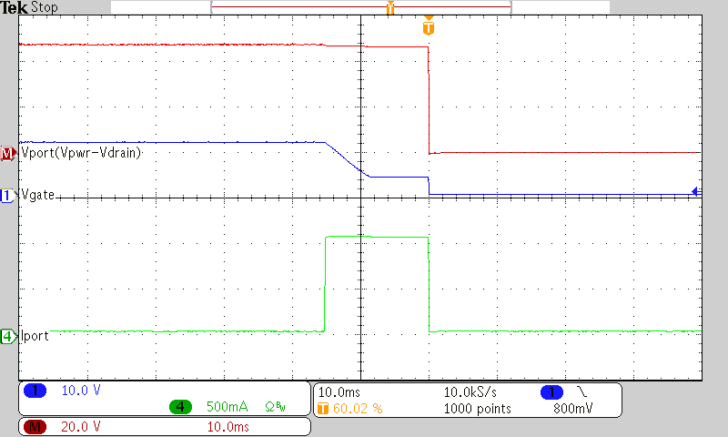
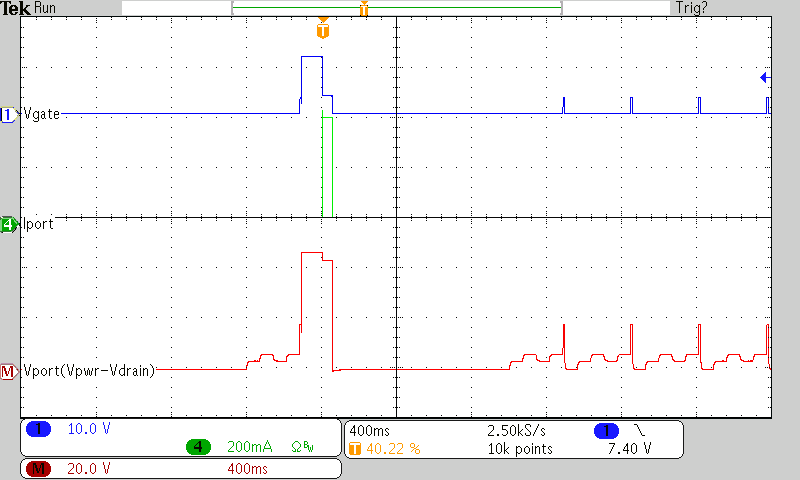
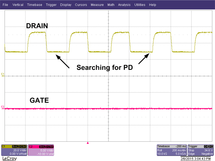 Figure 92. Detection With Open Circuit
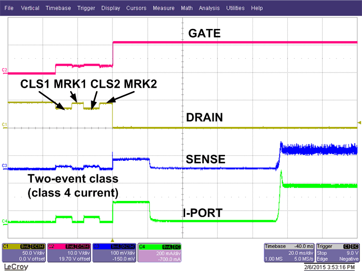 Figure 94. 2-Event Class and Port Turn On
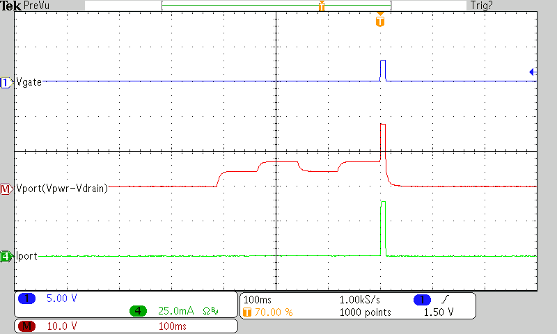
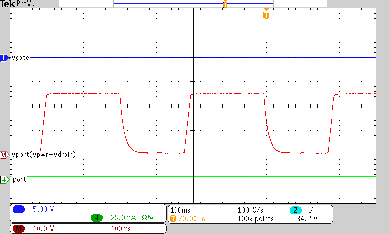
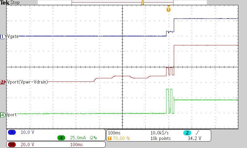
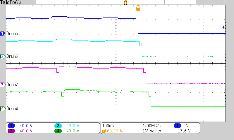
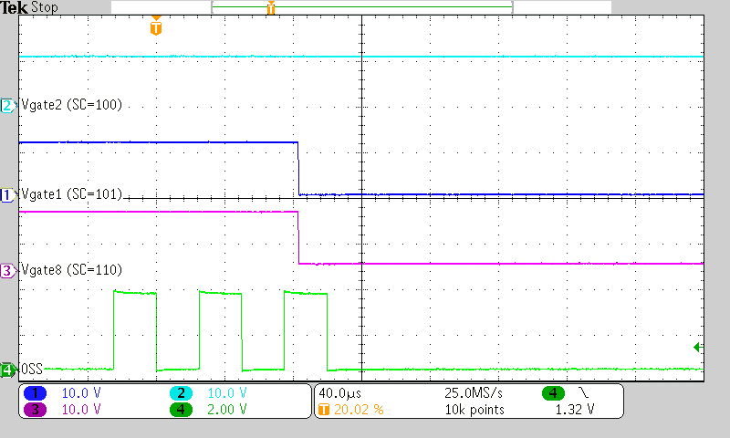
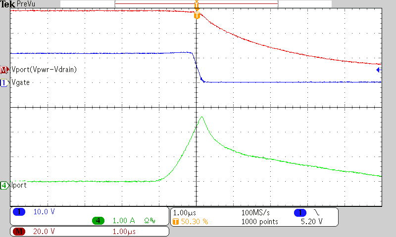
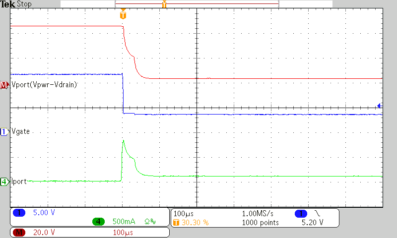
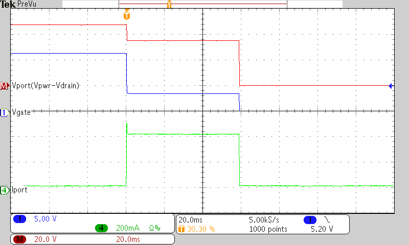
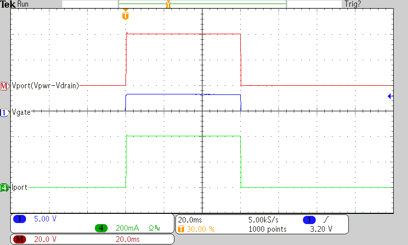
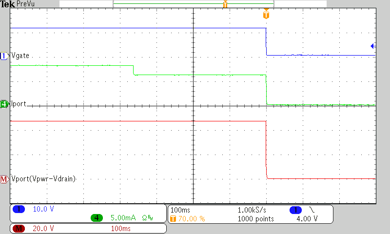
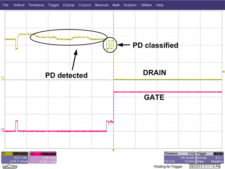 Figure 93. Detection, 2-Event Class and Port Turn On
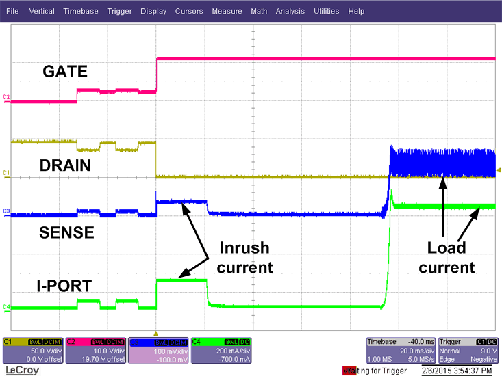 Figure 95. 2-Event Class and Port Turn On
