ZHCSGR0A February 2015 – August 2017 TPS2388
PRODUCTION DATA.
- 1 特性
- 2 应用
- 3 说明
- 4 修订历史记录
- 5 Pin Configuration and Functions
- 6 Specifications
- 7 Parameter Measurement Information
-
8 Detailed Description
- 8.1 Overview
- 8.2 Functional Block Diagram
- 8.3 Feature Description
- 8.4 Device Functional Modes
- 8.5 Programming
- 8.6
Register Maps
- 8.6.1 Complete Register Set
- 8.6.2 INTERRUPT Register
- 8.6.3 INTERRUPT MASK Register
- 8.6.4 POWER EVENT Register
- 8.6.5 DETECTION EVENT Register
- 8.6.6 FAULT EVENT Register
- 8.6.7 START/ILIM EVENT Register
- 8.6.8 SUPPLY EVENT Register
- 8.6.9 PORT 1 STATUS Register
- 8.6.10 PORT 2 STATUS Register
- 8.6.11 PORT 3 STATUS Register
- 8.6.12 PORT 4 STATUS Register
- 8.6.13 POWER STATUS Register
- 8.6.14 Pin Status Register
- 8.6.15 OPERATING MODE Register
- 8.6.16 DISCONNECT ENABLE Register
- 8.6.17 DETECT/CLASS ENABLE Register
- 8.6.18 Port Power Priority/ICUT Disable Register Name
- 8.6.19 TIMING CONFIGURATION Register
- 8.6.20 GENERAL MASK Register
- 8.6.21 DETECT/CLASS RESTART Register
- 8.6.22 POWER ENABLE Register
- 8.6.23 RESET Register
- 8.6.24 ID Register
- 8.6.25 Police 21 Configuration Register
- 8.6.26 Police 43 Configuration Register
- 8.6.27 IEEE Power Enable Register
- 8.6.28 Power-on Fault Register
- 8.6.29 PORT RE-MAPPING Register
- 8.6.30 Port 21 Multi Bit Priority Register
- 8.6.31 Port 43 Multi Bit Priority Register
- 8.6.32 TEMPERATURE Register
- 8.6.33 INPUT VOLTAGE Register
- 8.6.34 PORT 1 CURRENT Register
- 8.6.35 PORT 2 CURRENT Register
- 8.6.36 PORT 3 CURRENT Register
- 8.6.37 PORT 4 CURRENT Register
- 8.6.38 PORT 1 VOLTAGE Register
- 8.6.39 PORT 2 VOLTAGE Register
- 8.6.40 PORT 3 VOLTAGE Register
- 8.6.41 PORT 4 VOLTAGE Register
- 8.6.42 PoE Plus Register
- 8.6.43 FIRMWARE REVISION
- 8.6.44 I2C WATCHDOG Register
- 8.6.45 DEVICE ID Register
- 8.6.46 PORT 1 DETECT RESISTANCE Register
- 8.6.47 PORT 2 DETECT RESISTANCE Register
- 8.6.48 PORT 3 DETECT RESISTANCE Register
- 8.6.49 PORT 4 DETECT RESISTANCE Register
- 9 Application and Implementation
- 10Power Supply Recommendations
- 11Layout
- 12器件和文档支持
- 13机械、封装和可订购信息
11 Layout
11.1 Layout Guidelines
11.1.1 Port Current Kelvin Sensing
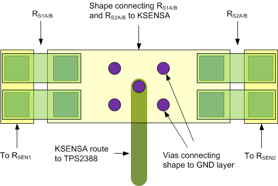
KSENSA is shared between SEN1 and SEN2, KSENSB is shared between SEN3 and SEN4, KSENSC is shared between SEN5 and SEN6, and KSENSD is shared between SEN7 and SEN8. To optimize the accuracy of the measurement, the PCB layout must be done carefully to minimize impact of PCB trace resistance. Refer to as an example.
 Figure 96. Kelvin Sense Layout Example
11.2 Layout Example
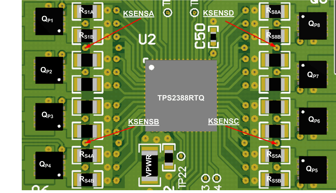
 Figure 97. Eight Port Layout Example (Top Side)
11.2.1 Component Placement and Routing Guidelines
11.2.1.1 Power Pin Bypass Capacitors
11.2.1.2 Per-Port Components
- RSnA / RSnB: Place according to in a manner that facilitates a clean Kelvin connection with KSENSEA/B/C/D.
- QPn: Place QPn around the TPS2388 as illustrated in Figure 97. Provide sufficient copper from QPn drain to FPn.
- FPn, CPn, DPnA, DPnB: Place this circuit group near the RJ45 port connector (or port power interface if a daughter board type of interface is used as illustrated in Figure 97). Connect this circuit group to QPn drain or GND (TPS2388- AGND) using low inductance traces.