ZHCSHW5A September 2017 – December 2017 TPS23521
PRODUCTION DATA.
- 1 特性
- 2 应用
- 3 说明
- 4 修订历史记录
- 5 Pin Configuration and Functions
- 6 Specifications
- 7 Parameter Measurement Information
- 8 Detailed Description
-
9 Application and Implementation
- 9.1 Application Information
- 9.2
Typical Application
- 9.2.1 Design Requirements
- 9.2.2
Detailed Design Procedure
- 9.2.2.1 Selecting RSNS
- 9.2.2.2 Selecting Soft Start Setting: CSS and CSS,VEE
- 9.2.2.3 Selecting VDS Switch Over Threshold
- 9.2.2.4 Timer Selection
- 9.2.2.5 MOSFET Selection and SOA Checks
- 9.2.2.6 EMI Filter Consideration
- 9.2.2.7 Under Voltage and Over Voltage Settings
- 9.2.2.8 Choosing RVCC and CVCC
- 9.2.2.9 Power Good Interface to Downstream DC/DC
- 9.2.3 Application Curves
- 10Power Supply Recommendations
- 11Layout
- 12器件和文档支持
- 13机械、封装和可订购信息
9.2.2.5 MOSFET Selection and SOA Checks
When selecting MOSFETs for the –48 V application the three key parameters are: VDS rating, RDSON, and safe operating area (SOA). For this application the PSMN4R8-100BSE was selected as the Main hot swap FET (Q1) to provide a 100 V VDS rating, low RDSON, and great SOA. Since this is a high power application 2 CSD19532Q5B FETs were used as auxiliary FETs (Q2) to reduce steady state power dissipation. After selecting the MOSFET, it is important to double check that it has sufficient SOA to handle the key stress scenarios: start-up, output Hot Short, and Start into Short. MOSFET's SOA is usually specified at a case temperature of 25°C and should be derated based on the maximum case temperature expected in the application.
First, compute how much current will flow through Q1 using a current division formula shown below. For this example the FET RDSON at 100°C was used. RDSON of Q1 (RDSON1) is 4.8 mΩ (PSMNR8-100BSE max RDSON at 25°C) x 1.8 (temperature coefficient), which equals 8.64 mΩ. RDSON of Q2 (RDSON2) is 4.9 mΩ (CSD19532Q5B max RDSON at 25°C) x 1.6 (temperature coefficient), which equals 7.84 mΩ.

Next the maximum temperature of Q1 can be computed using the equations below.


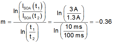
Next the stress the MOSFET will experience during operation should be compared to the FETs capability. First, consider the power up. The inrush current with max COUT will be 0.53 A and the inrush will last for 198 ms. Note that the power dissipation of the FET will start at VIN,MAX × IINR and reduce to zero as the VDS of the MOSFET is reduced. The SOA curve of a typical MOSFET assume the same power dissipation for a given time. A conservative approach is to assume an equivalent power profile where PFET = VIN,MAX × IINR for t = Tstart-up /2. In this instance, the SOA can be checked by looking at a 72 V, 0.53 A, 99 ms pulse. Based on the SOA of the PSMN4R8-100BSE, it can handle 72 V, 3 A for 10 ms and it can handle 72 V, 1.3 A for 100 ms. The SOA at TC = 25°C for 99 ms can be extrapolated by approximating SOA vs time as a power function as shown in equations below:


Finally, the FET SOA needs to be derated based on the maximum case temperature as shown below. Note that the FET can handle 0.79 A, while it will have 0.53 A during start-up. Thus there is a lot of margin during this test condition.

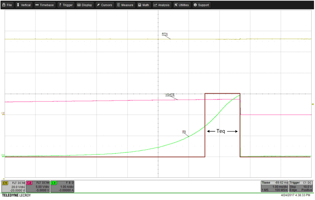
A similar approach should be taken to compute the FETs SOA capability during a Hot Short and start into short. As shown in the following figure, during a start into short the gate is coming up very slowly due to a large capacitance tied to the gate through the SS pin. Thus it is more stressful than a Hot Short and should be used for worst case SOA calculations. To compare the FET stress during start-up into short to the SOA curves the stress needs to be approximated as a square pulse as showing in the figure below. In this example, the stress is approximated with a 1.3 ms (Teq), 3 A, 72 V pulse. The FET can handle 18 A, 72 V for 1 ms and 3 A, 72 V for 10 ms. Using approximation and temp derating as shown earlier, the FET's capability can be computed as 8.9 A, 72 V, for 1.3 ms at 83.7°C. 8.9 A is significantly larger than 3 A implying great margin.
 Figure 13. Teq During a Start Into a Short
The final operating point to check is the operation with high current and VDS just below the VDS,SW threshold. In this example, the time out would be 1.1ms (one half of the time out at Vd = 0 V), the current will be 40 A, and the voltage would be 20 V. Looking up the SOA curve, the FET can handle 100 A, 20 V for 1 ms and 40 A, 20 V for 10 ms. Repeating previously shown approximations and temp derating, the FET's capability is computed to be 58 A, 20 V, for 1.1 ms at 83.7°C. Again this is below the worst case operating point of 40 A and 20 V suggesting good margin.