ZHCSCL1A June 2014 – June 2014 TPS22962
PRODUCTION DATA.
9 Applications and Implementation
9.1 Application Information
This section will highlight some of the design considerations when implementing this device in various applications. A PSPICE model for this device is also available in the product page of this device on www.ti.com for further aid.
9.2 Typical Application
This application demonstrates how the TPS22962 can be used to power downstream modules with large capacitances. The example below is powering a 100-µF capacitive output load.
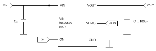 Figure 32. Typical Application Schematic for Powering a Downstream Module
9.2.1 Design Requirements
For this design example, use the following as the input parameters.
Table 2. Design Parameters
| DESIGN PARAMETER | EXAMPLE VALUE |
|---|---|
| VIN | 5.0 V |
| VBIAS | 5.0 V |
| Load current | 10 A |
9.2.2 Detailed Design Procedure
To begin the design process, the designer needs to know the following:
- VIN voltage
- VBIAS voltage
- Load current
9.2.2.1 VIN to VOUT Voltage Drop
The VIN to VOUT voltage drop in the device is determined by the RON of the device and the load current. The RON of the device depends upon the VIN and VBIAS conditions of the device. Refer to the RON specification of the device in the Electrical Characteristics table of this datasheet. Once the RON of the device is determined based upon the VIN and VBIAS conditions, use Equation 1 to calculate the VIN to VOUT voltage drop:

where
- ΔV = voltage drop from VIN to VOUT
- ILOAD = load current
- RON = On-resistance of the device for a specific VIN and VBIAS combination
An appropriate ILOAD must be chosen such that the IMAX specification of the device is not violated.
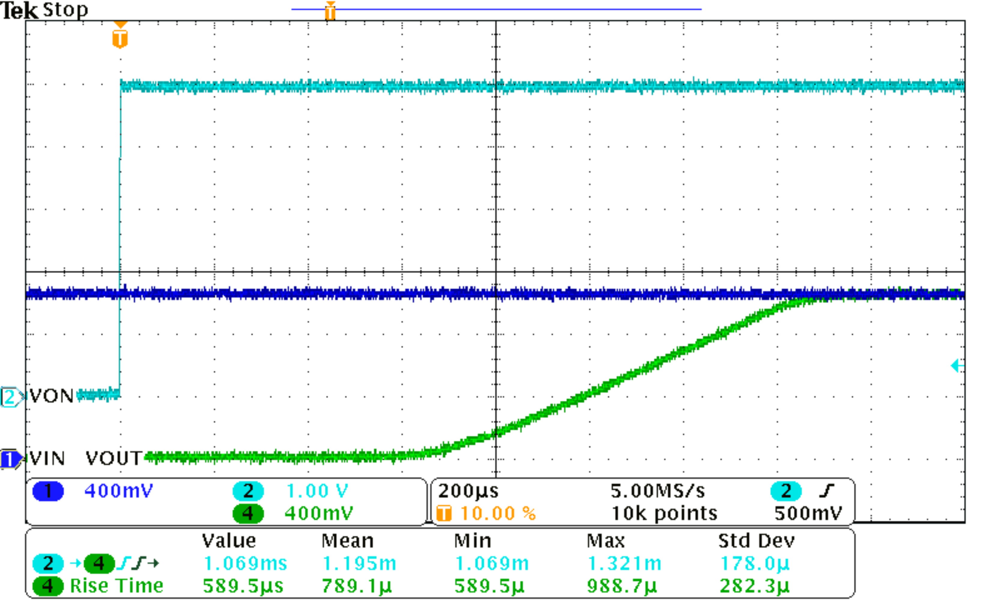
9.2.2.2 Inrush Current
To determine how much inrush current will be caused by the CL capacitor, use Equation 2:

where
- IINRUSH = amount of inrush caused by CL
- CL = capacitance on VOUT
- dt = time it takes for change in VOUT during the ramp up of VOUT when the device is enabled
- dVOUT = change in VOUT during the ramp up of VOUT when the device is enabled
An appropriate CL value should be placed on VOUT such that the IMAX and IPLS specficiations of the device are not violated.
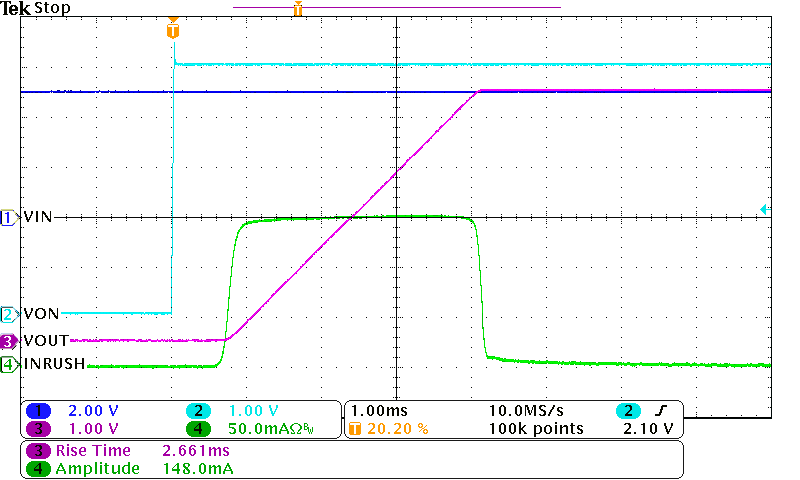 Figure 33. Inrush Current (VBIAS = 5 V, VIN = 5 V, CL = 100 µF)
9.2.2.3 Thermal Considerations
The maximum IC junction temperature should be restricted to 125°C under normal operating conditions. To calculate the maximum allowable dissipation, PD(max) for a given output current and ambient temperature, use Equation 3.
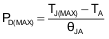
where
- PD(max) = maximum allowable power dissipation
- TJ(max) = maximum allowable junction temperature (125°C for the TPS22962)
- TA = ambient temperature of the device
- θJA = junction to air thermal impedance. See Thermal Information section. This parameter is highly dependent upon board layout.
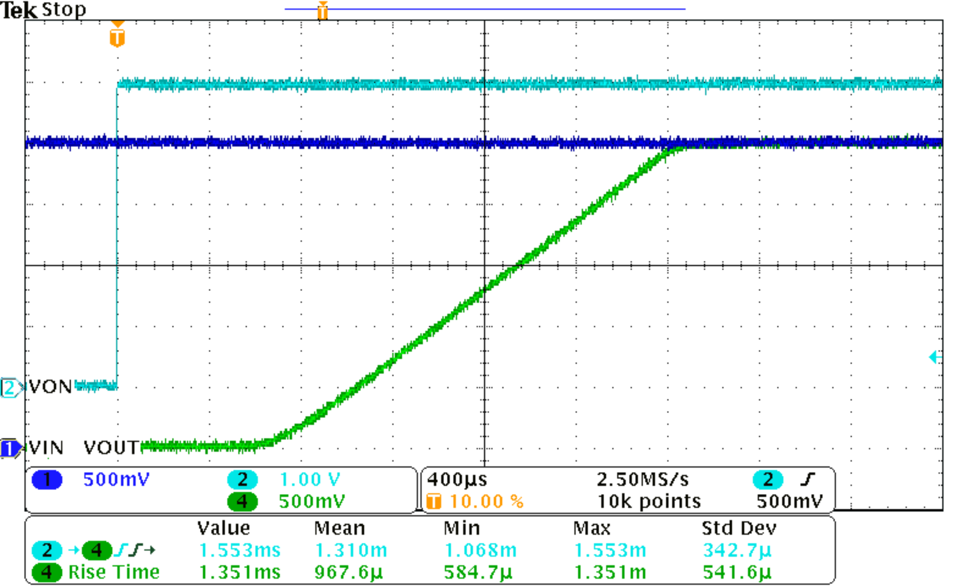
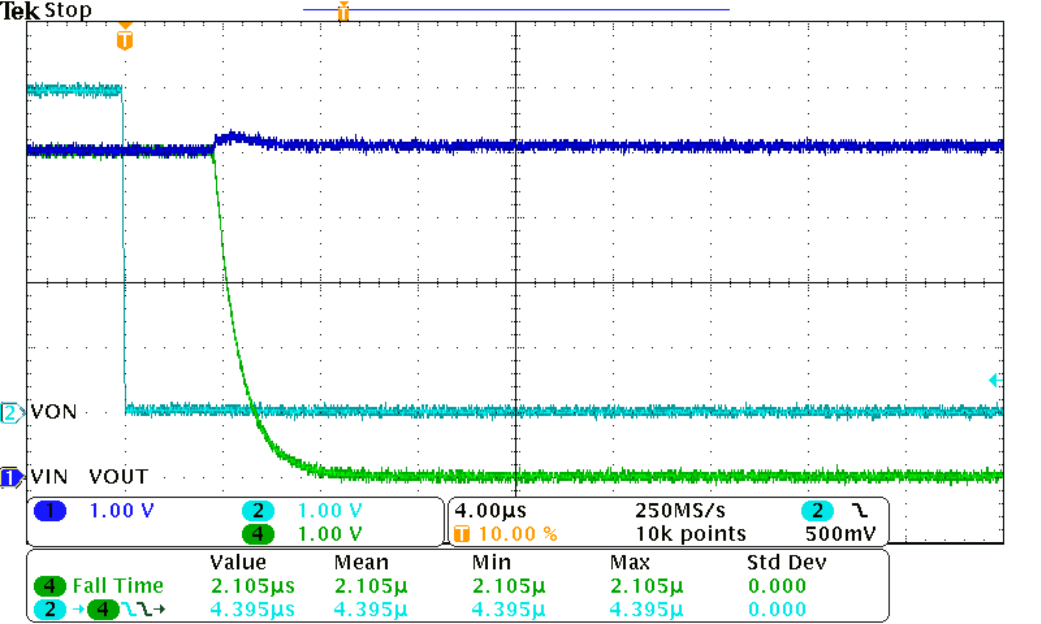
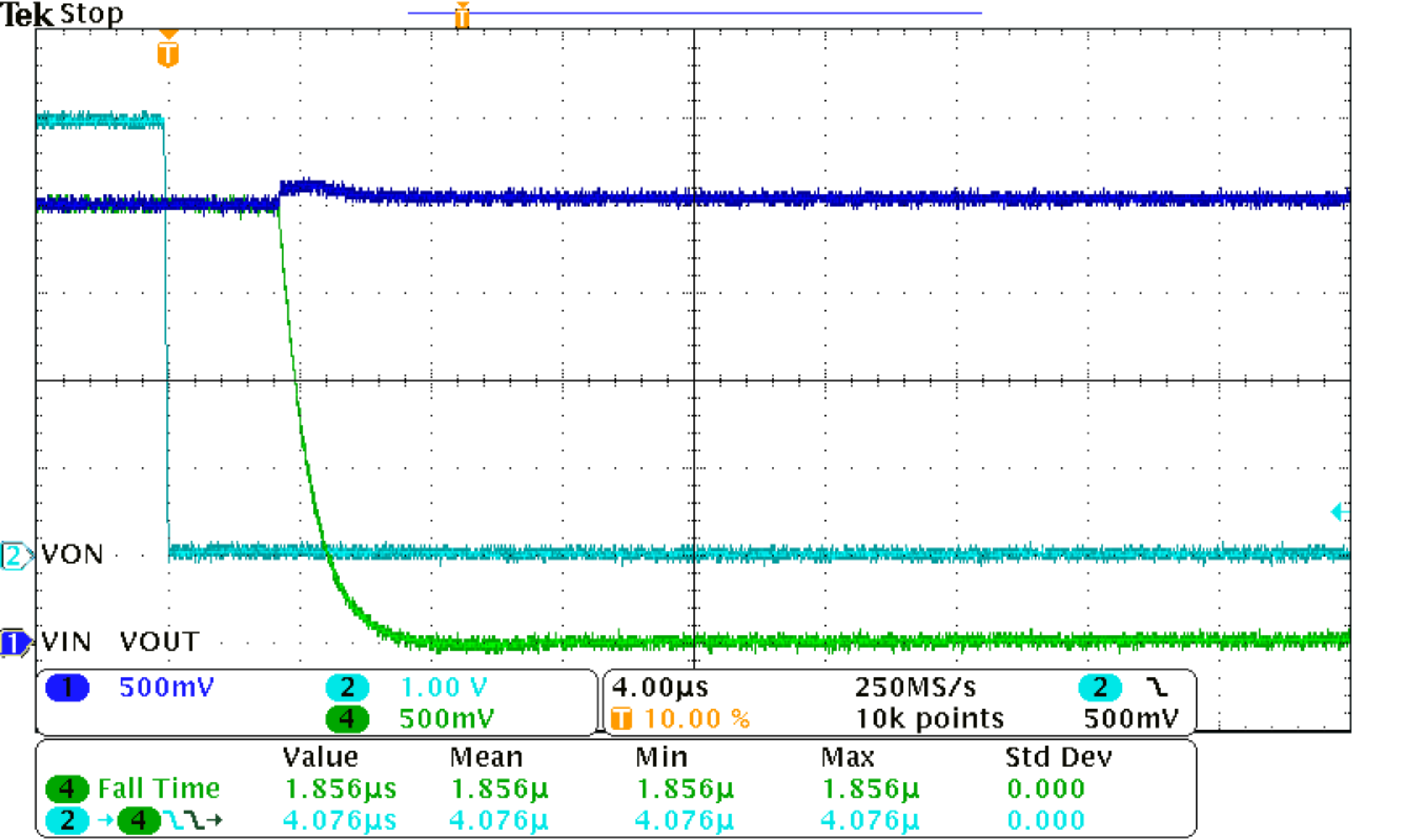
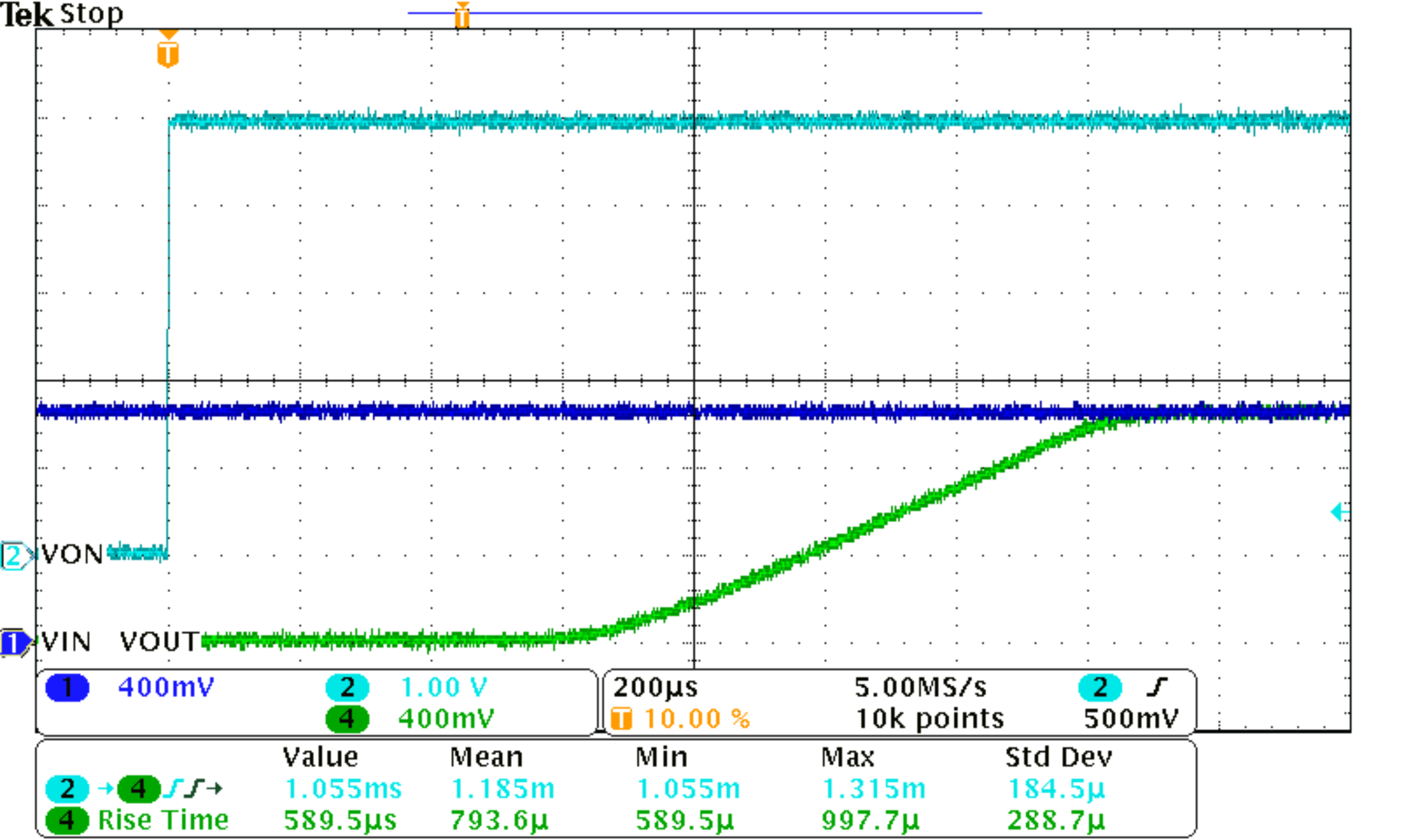
9.2.3 Application Curves
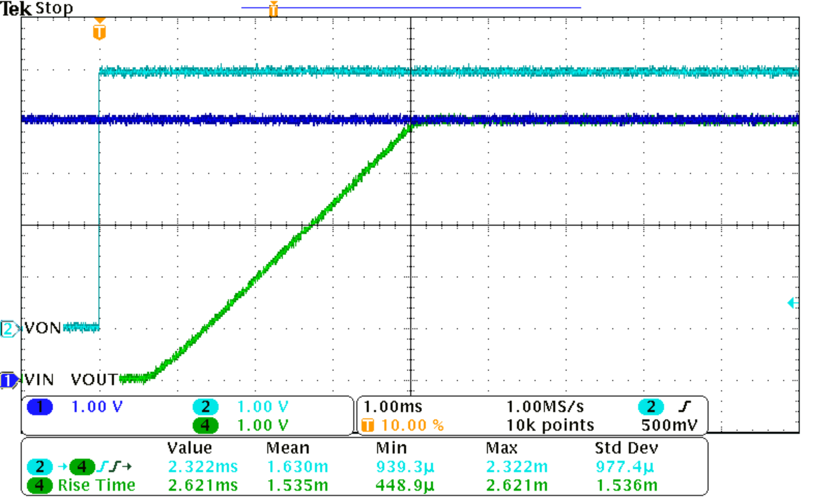
| VBIAS = 5 V | VIN = 5 V | CIN = 1 µF |
| CL = 0.1 µF |
| VBIAS = 2.5 V | VIN = 2.5 V | CIN = 1 µF |
| CL = 0.1 µF |
| VBIAS = 5 V | VIN = 5 V | CIN = 1 µF |
| CL = 0.1 µF |
| VBIAS = 2.5 V | VIN = 2.5 V | CIN = 1 µF |
| CL = 0.1 µF |
| VBIAS = 5 V | VIN = 1.05 V | CIN = 1 µF |
| CL = 0.1 µF |
| VBIAS = 2.5 V | VIN = 1.05 V | CIN = 1 µF |
| CL = 0.1 µF |
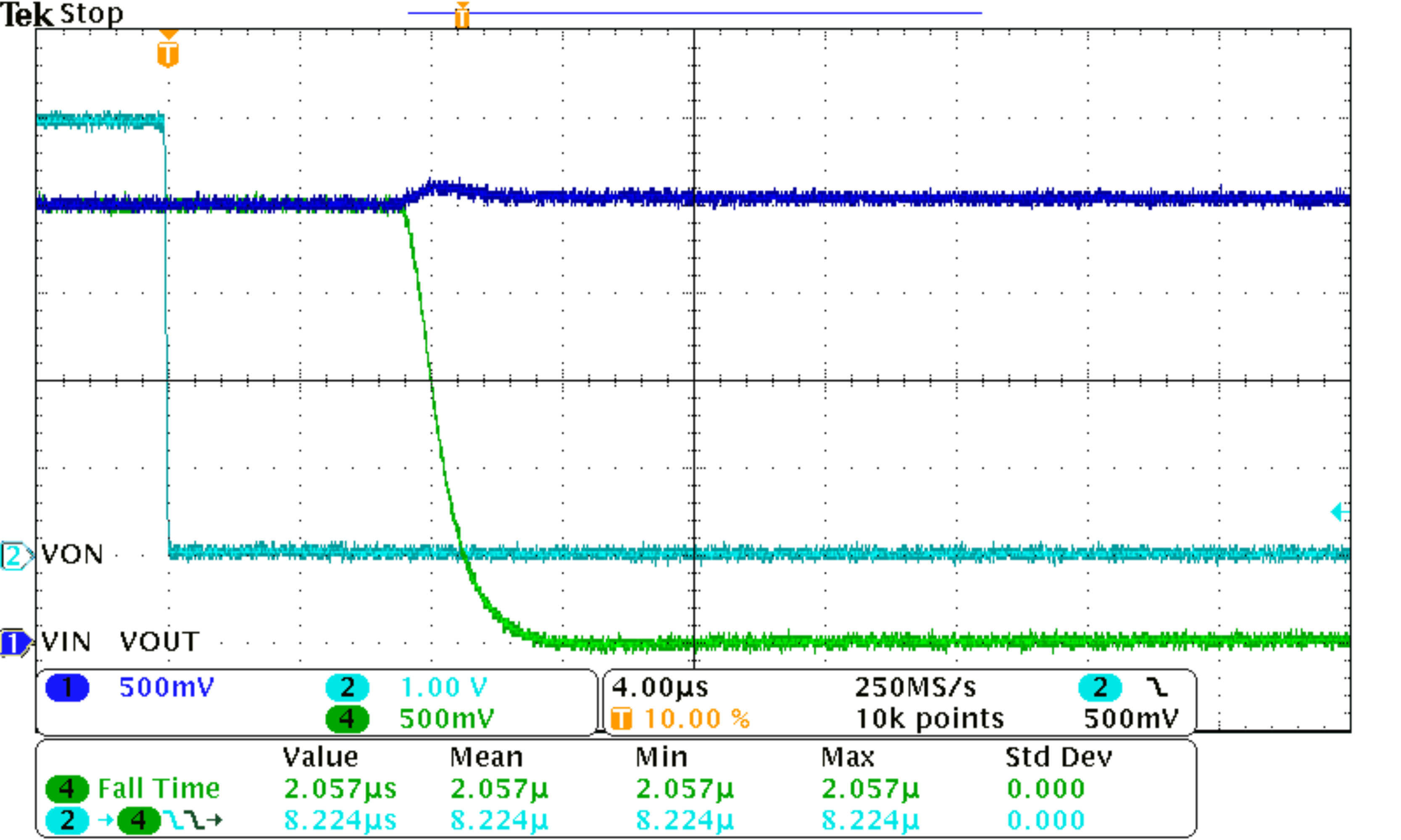
| VBIAS = 5 V | VIN = 2.5 V | CIN = 1 µF |
| CL = 0.1 µF |
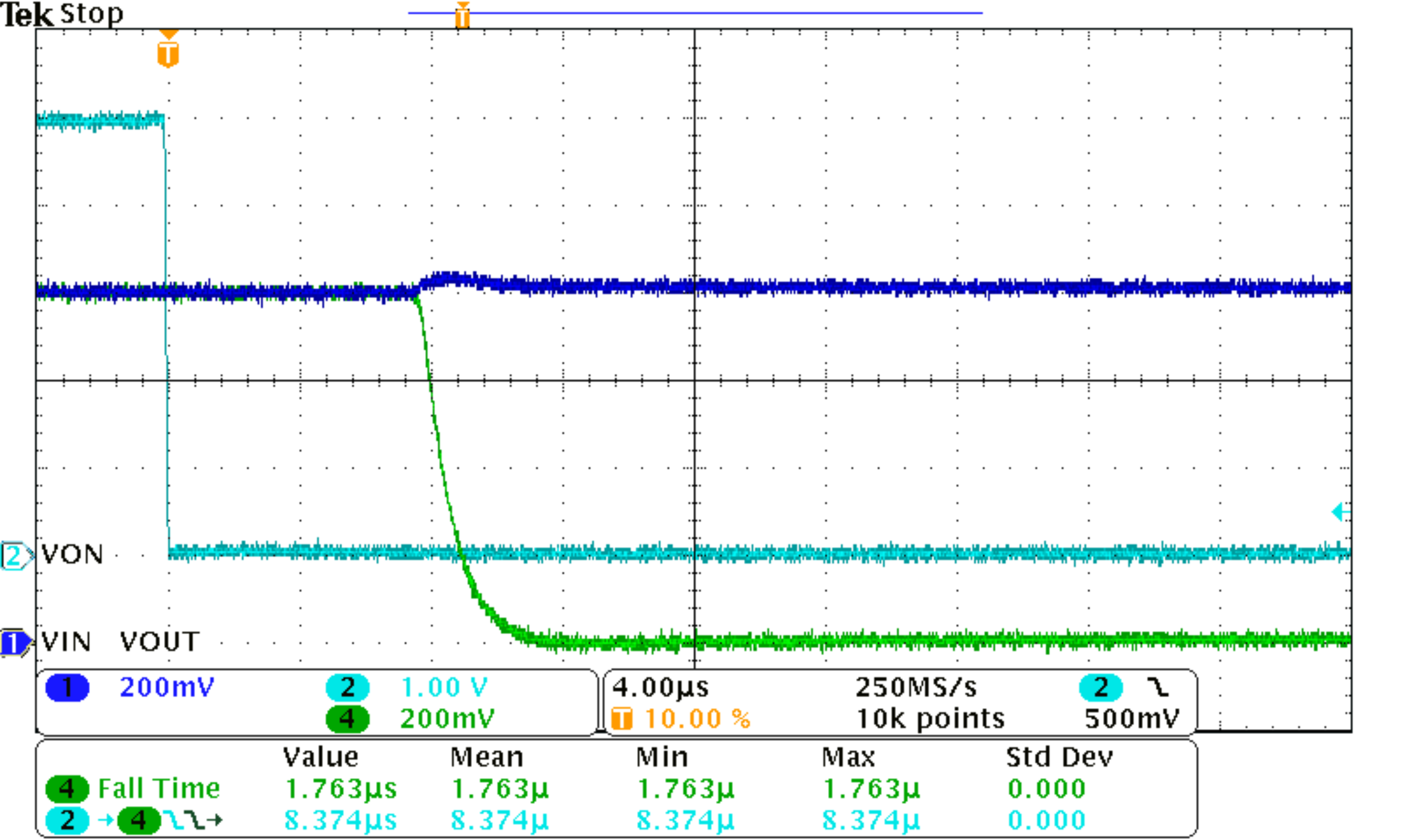
| VBIAS = 2.5 V | VIN = 0.8 V | CIN = 1 µF |
| CL = 0.1 µF |