ZHCSCL1A June 2014 – June 2014 TPS22962
PRODUCTION DATA.
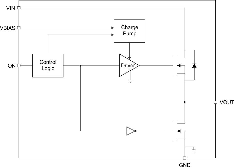
8 Detailed Description
8.1 Overview
The device is a 5.5 V, 10 A load switch in a 8-pin SON package. To reduce voltage drop for low voltage and high current rails, the device implements an ultra-low resistance N-channel MOSFET which reduces the drop out voltage through the device.
The device has a controlled and fixed slew rate which helps reduce or eliminate power supply droop due to large inrush currents. During shutdown, the device has very low leakage currents, thereby reducing unnecessary leakages for downstream modules during standby. Integrated control logic, driver, charge pump, and output discharge FET eliminates the need for any external components, which reduces solution size and bill of materials (BOM) count.
8.2 Functional Block Diagram
8.3 Feature Description
8.3.1 On/off Control
The ON pin controls the state of the load switch, and asserting the pin high (active high) enables the switch. The ON pin is compatible with standard GPIO logic threshold and can be used with any microcontroller or discrete logic with 1.2-V or higher GPIO voltage. This pin cannot be left floating and must be tied either high or low for proper functionality.
8.3.2 Input Capacitor (CIN)
To limit the voltage drop on the input supply caused by transient in-rush currents when the switch turns on into a discharged load capacitor or short-circuit, a capacitor needs to be placed between VIN and GND. A 1-µF ceramic capacitor, CIN, placed close to the pins, is usually sufficient. Higher values of CIN can be used to further reduce the voltage drop in high-current application. When switching heavy loads, it is recommended to have an input capacitor 10 times higher than the output capacitor to avoid excessive voltage drop; however, a 10 to 1 ratio for capacitance is not required for proper functionality of the device, but a ratio smaller than 10 to 1 (such as 1 to 1) could cause a VIN dip upon turn-on due to inrush currents based on external factor such as board parasitics and output bulk capacitance.
8.3.3 Output Capacitor (CL)
Due to the integrated body diode in the N-channel MOSFET, a CIN greater than CL is highly recommended. A CL greater than CIN can cause VOUT to exceed VIN when the system supply is removed. This could result in current flow through the body diode from VOUT to VIN. A CIN to CL ratio of 10 to 1 is recommended for minimizing VIN dip caused by inrush currents during startup, however a 10 to 1 ratio for capacitance is not required for proper functionality of the device. A ratio smaller than 10 to 1 (such as 1 to 1) could cause a VIN dip upon turn-on due to inrush currents based on external factor such as board parasitics and output bulk capacitance.
8.3.4 VIN and VBIAS Voltage Range
For optimal RON performance, make sure VIN ≤ VBIAS. The device may still be functional if VIN > VBIAS but it will exhibit RON greater than what is listed in the Electrical Characteristics table. See Figure 31 for an example of a typical device. Notice the increasing RON as VIN increases. Be sure to never exceed the maximum voltage rating for VIN and VBIAS. Performance of the device is not guaranteed for VIN > VBIAS.
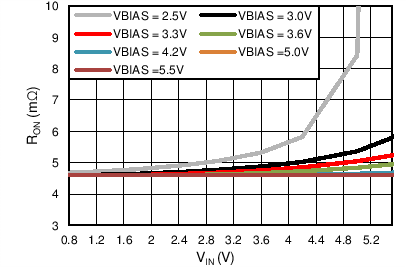 Figure 31. RON vs VIN (VIN > VBIAS)
8.4 Device Functional Modes
Table 1 shows the connection of VOUT depending on the state of the ON pin.
Table 1. VOUT Connection
| ON | VOUT |
|---|---|
| L | GND |
| H | VIN |