ZHCSCL1A June 2014 – June 2014 TPS22962
PRODUCTION DATA.
7 Specifications
7.1 Absolute Maximum Ratings
Over operating free-air temperature range (unless otherwise noted)(1)| MIN | MAX | UNIT | ||
|---|---|---|---|---|
| VIN | Input voltage range | –0.3 | 6 | V |
| VBIAS | Bias voltage range | –0.3 | 6 | V |
| VOUT | Output voltage range | –0.3 | 6 | V |
| VON | ON pin voltage range | –0.3 | 6 | V |
| IMAX | Maximum Continuous Switch Current, TA = 70°C | 10 | A | |
| IPLS | Maximum Pulsed Switch Current, pulse < 300 µs, 2% duty cycle | 12 | A | |
| TJ | Maximum junction temperature | 125 | °C |
(1) Stresses beyond those listed under Absolute Maximum Ratings may cause permanent damage to the device. These are stress ratings only, which do not imply functional operation of the device at these or any other conditions beyond those indicated under Recommended Operating Conditions. Exposure to absolute-maximum-rated conditions for extended periods may affect device reliability.
7.2 Handling Ratings
| MIN | MAX | UNIT | |||
|---|---|---|---|---|---|
| Tstg | Storage temperature range | –65 | 150 | °C | |
| V(ESD) | Electrostatic discharge | Human body model (HBM), per ANSI/ESDA/JEDEC JS-001, all pins(1) | 0 | 2 | kV |
| Charged device model (CDM), per JEDEC specification JESD22-C101, all pins(2) | 0 | 1 | |||
(1) JEDEC document JEP155 states that 500-V HBM allows safe manufacturing with a standard ESD control process.
(2) JEDEC document JEP157 states that 250-V CDM allows safe manufacturing with a standard ESD control process.
7.3 Recommended Operating Conditions
Over operating free-air temperature range (unless otherwise noted)| MIN | MAX | UNIT | |||
|---|---|---|---|---|---|
| VIN | Input voltage range | 0.8 | VBIAS | V | |
| VBIAS | Bias voltage range | 2.5 | 5.5 | V | |
| VON | ON voltage range | 0 | 5.5 | V | |
| VOUT | Output voltage range | VIN | V | ||
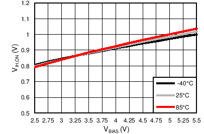
| VIH, ON | High-level voltage, ON | VBIAS = 2.5 V to 5.5 V | 1.2 | 5.5 | V |
| VIL, ON | Low-level voltage, ON | VBIAS = 2.5 V to 5.5 V | 0 | 0.5 | V |
| TA | Operating free-air temperature range | –40 | 85 | °C | |
| CIN | Input Capacitor | 1(1) | µF | ||
(1) Refer to Detailed Description section.
7.4 Thermal Information
| THERMAL METRIC(1) | TPS22962 | UNIT | |
|---|---|---|---|
| DNY 8 PINS |
|||
| RθJA | Junction-to-ambient thermal resistance | 44.6 | °C/W |
| RθJCtop | Junction-to-case (top) thermal resistance | 44.4 | |
| RθJB | Junction-to-board thermal resistance | 17.6 | |
| ψJT | Junction-to-top characterization parameter | 0.4 | |
| ψJB | Junction-to-board characterization parameter | 17.4 | |
| RθJCbot | Junction-to-case (bottom) thermal resistance | 1.1 | |
(1) For more information about traditional and new thermal metrics, see the IC Package Thermal Metrics application report, SPRA953.
7.5 Electrical Characteristics, VBIAS = 5.0 V
Unless otherwise noted, the specification in the following table applies over the operating ambient temperature–40°C ≤ TA ≤ 85°C (Full) and VBIAS = 5.0 V. Typical values are for TA = 25°C (unless otherwise noted).
| PARAMETER | TEST CONDITIONS | TA | MIN | TYP | MAX | UNIT | ||
|---|---|---|---|---|---|---|---|---|
| CURRENTS AND THRESHOLDS | ||||||||
| IQ, VBIAS | VBIAS quiescent current | IOUT = 0, VIN = VBIAS, VON = 5.0 V |
Full | 20.4 | 26.0 | µA | ||
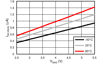
| ISD, VBIAS | VBIAS shutdown current | VON = 0 V, VOUT = 0 V | Full | 1.1 | 1.5 | µA | ||
| ISD, VIN | VIN shutdown current | VON = 0 V, VOUT = 0 V |
VIN = 5.0 V | Full | 0.1 | µA | ||
| VIN = 3.3 V | 0.1 | |||||||
| VIN = 1.8 V | 0.1 | |||||||
| VIN = 1.05 V | 0.1 | |||||||
| VIN = 0.8 V | 0.1 | |||||||
| ION | ON pin leakage current | VON = 5.5 V | Full | 0.1 | µA | |||
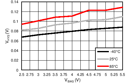
| VHYS, ON | ON pin hysteresis | VBIAS = VIN | 25°C | 113 | mV | |||
| RESISTANCE CHARACTERISTICS | ||||||||
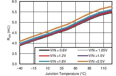
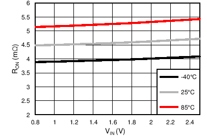
| RON | On-state resistance | IOUT = –200 mA, VBIAS = 5.0 V |
VIN = 5.0 V | 25°C | 4.4 | 5.0 | mΩ | |
| Full | 5.6 | |||||||
| VIN = 3.3 V | 25°C | 4.4 | 5.0 | mΩ | ||||
| Full | 5.6 | |||||||
| VIN = 2.5 V | 25°C | 4.4 | 5.0 | mΩ | ||||
| Full | 5.6 | |||||||
| VIN = 1.8 V | 25°C | 4.4 | 5.0 | mΩ | ||||
| Full | 5.6 | |||||||
| VIN = 1.05 V | 25°C | 4.4 | 5.0 | mΩ | ||||
| Full | 5.6 | |||||||
| VIN = 0.8 V | 25°C | 4.4 | 5.0 | mΩ | ||||
| Full | 5.6 | |||||||
| RPD | Output pulldown resistance | VIN = 5.0 V, VON = 0 V, VOUT = 1 V | Full | 224 | 233 | Ω | ||
7.6 Electrical Characteristics, VBIAS = 2.5 V
Unless otherwise noted, the specification in the following table applies over the operating ambient temperature–40°C ≤ TA ≤ 85°C (Full) and VBIAS = 2.5 V. Typical values are for TA = 25°C unless otherwise noted.
| PARAMETER | TEST CONDITIONS | TA | MIN | TYP | MAX | UNIT | ||
|---|---|---|---|---|---|---|---|---|
| CURRENTS AND THRESHOLDS | ||||||||
| IQ, VBIAS | VBIAS quiescent current | IOUT = 0, VIN = VBIAS, VON = 5.0 V |
Full | 9.9 | 12.5 | µA | ||
| ISD, VBIAS | VBIAS shutdown current | VON = 0 V, VOUT = 0 V | Full | 0.5 | 0.65 | µA | ||
| ISD, VIN | VIN shutdown current | VON = 0 V, VOUT = 0 V |
VIN = 2.5 V | Full | 0.1 | µA | ||
| VIN = 1.8 V | 0.1 | |||||||
| VIN = 1.05 V | 0.1 | |||||||
| VIN = 0.8 V | 0.1 | |||||||
| ION | ON pin input leakage current | VON = 5.5 V | Full | 0.1 | µA | |||
| VHYS, ON | ON pin hysteresis | VBIAS = VIN | 25°C | 83 | mV | |||
| RESISTANCE CHARACTERISTICS | ||||||||
| RON | On-state resistance | IOUT = –200 mA, VBIAS = 2.5 V |
VIN =2.5 V | 25°C | 4.7 | 5.3 | mΩ | |
| Full | 6.0 | |||||||
| VIN =1.8 V | 25°C | 4.6 | 5.2 | mΩ | ||||
| Full | 5.8 | |||||||
| VIN =1.05 V | 25°C | 4.5 | 5.1 | mΩ | ||||
| Full | 5.7 | |||||||
| VIN = 0.8 V | 25°C | 4.5 | 5.1 | mΩ | ||||
| Full | 5.7 | |||||||
| RPD | Output pulldown resistance | VIN = 2.5 V, VON = 0 V, VOUT = 1 V | Full | 224 | 233 | Ω | ||
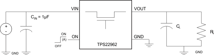
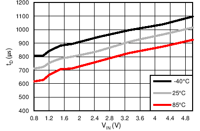
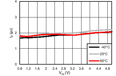
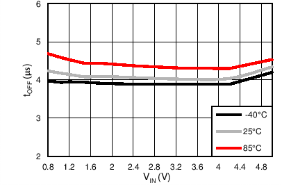
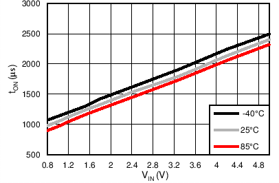
7.7 Switching Characteristics
Refer to the timing test circuit in Figure 1 (unless otherwise noted) for references to external components used for the test condition in the switching characteristics table. Switching characteristics shown below are only valid for the power-up sequence where VIN and VBIAS are already in steady state condition before the ON pin is asserted high.| PARAMETER | TEST CONDITION | MIN | TYP | MAX | UNIT | |
|---|---|---|---|---|---|---|
| VIN = 5 V, VON = VBIAS = 5 V, TA = 25ºC (unless otherwise noted) | ||||||
| tON | Turn-on time | RL = 10 Ω, CL = 0.1 µF | 2397 | µs | ||
| tOFF | Turn-off time | 4 | ||||
| tR | VOUT rise time | 2663 | ||||
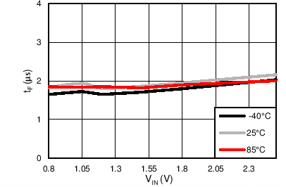
| tF | VOUT fall time | 2 | ||||
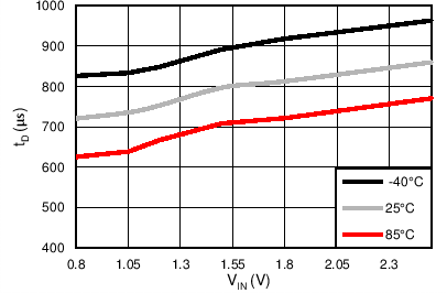
| tD | Delay time | 1009 | ||||
| VIN = 3.3 V, VON = VBIAS = 5 V, TA = 25ºC (unless otherwise noted) | ||||||
| tON | Turn-on time | RL = 10 Ω, CL = 0.1 µF | 1811 | µs | ||
| tOFF | Turn-off time | 4 | ||||
| tR | VOUT rise time | 1756 | ||||
| tF | VOUT fall time | 2 | ||||
| tD | Delay time | 897 | ||||
| VIN = 0.8 V, VON = VBIAS = 5 V, TA = 25ºC (unless otherwise noted) | ||||||
| tON | Turn-on time | RL = 10 Ω, CL = 0.1 µF | 981 | µs | ||
| tOFF | Turn-off time | 4 | ||||
| tR | VOUT rise time | 500 | ||||
| tF | VOUT fall time | 2 | ||||
| tD | Delay time | 714 | ||||
| VIN = 2.5 V, VON = 5 V, VBIAS = 2.5 V, TA = 25ºC (unless otherwise noted) | ||||||
| tON | Turn-on time | RL = 10Ω, CL = 0.1 µF | 1576 | µs | ||
| tOFF | Turn-off time | 8 | ||||
| tR | VOUT rise time | 1372 | ||||
| tF | VOUT fall time | 2 | ||||
| tD | Delay time | 865 | ||||
| VIN = 1.8V, VON = 5 V, VBIAS = 2.5 V, TA = 25ºC (unless otherwise noted) | ||||||
| tON | Turn-on time | RL = 10 Ω, CL = 0.1 µF | 1343 | µs | ||
| tOFF | Turn-off time | 7 | ||||
| tR | VOUT rise time | 1006 | ||||
| tF | VOUT fall time | 2 | ||||
| tD | Delay time | 815 | ||||
| VIN = 0.8 V, VON = 5V, VBIAS = 2.5 V, TA = 25ºC (unless otherwise noted) | ||||||
| tON | Turn-on time | RL = 10 Ω, CL = 0.1 µF | 994 | µs | ||
| tOFF | Turn-off time | 8 | ||||
| tR | VOUT rise time | 502 | ||||
| tF | VOUT fall time | 2 | ||||
| tD | Delay time | 723 | ||||
1. Rise and fall times of the control signal is 100ns.
Figure 1. Test Circuit
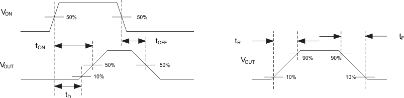 Figure 2. Timing Waveforms
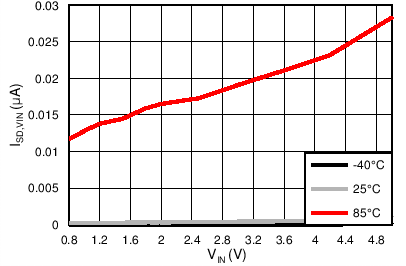
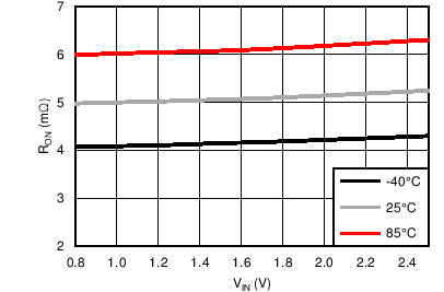
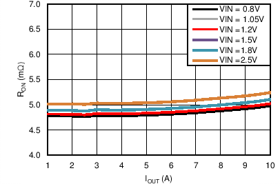
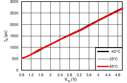
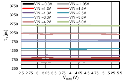
7.8 Typical Characteristics
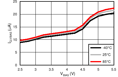
| VIN = VBIAS | VON = 5 V | IOUT = 0 A |
| VBIAS = 5 V | VON = 0 V | VOUT = 0 V |
| VBIAS = 5 V | VON = 5 V | IOUT = –200 mA |
| VBIAS = 5 V | VON = 5 V | IOUT = –200 mA |
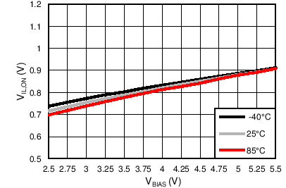
| VON = 0 V | VIN = 1.05 V | VOUT = 1 V |
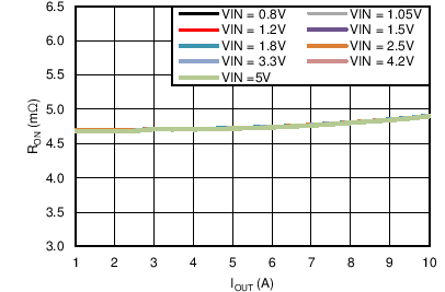
| VBIAS = 5 V | VON = 5 V | IOUT = –10 A |
| VBIAS = 5 V | VON = 5 V | TA = 25°C |
| VIN = VBIAS | IOUT = 0 A | |
| VBIAS = 2.5 V | RL = 10 Ω | CL = 0.1 µF |
| VBIAS = 2.5 V | RL = 10 Ω | CL = 0.1 µF |
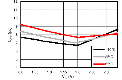
| VBIAS = 2.5 V | RL = 10 Ω | CL = 0.1 µF |
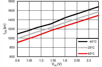
| VBIAS = 2.5 V | RL = 10 Ω | CL = 0.1 µF |
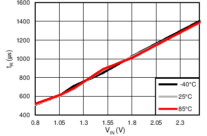
| VBIAS = 2.5 V | RL = 10 Ω | CL = 0.1 µF |
| TA = 25°C | RL = 10 Ω | CL = 0.1 µF |
| VIN = VBIAS | VON = 0 V | VOUT = 0 V |
| VBIAS = 2.5 V | VON = 5 V | IOUT = –200 mA |
| VBIAS = 2.5 V | VON = 5 V | IOUT = –200 mA |
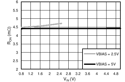
| TA = 25°C | VON = 5 V | IOUT = –200 mA |
| VBIAS = 2.5 V | VON = 5 V | IOUT = –10 A |
| VBIAS = 2.5 V | VON = 5 V | TA = 25°C |
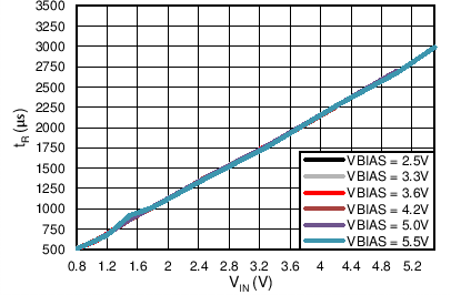
| VIN = VBIAS | ||
| VIN = VBIAS | IOUT = 0 A | |
| VBIAS = 5 V | RL = 10 Ω | CL = 0.1 µF |
| VBIAS = 5 V | RL = 10 Ω | CL = 0.1 µF |
| VBIAS = 5 V | RL = 10 Ω | CL = 0.1 µF |
| VBIAS = 5 V | RL = 10 Ω | CL = 0.1 µF |
| VBIAS = 5 V | RL = 10 Ω | CL = 0.1 µF |
| TA = 25°C | RL = 10 Ω | CL = 0.1 µF |