ZHCSCL1A June 2014 – June 2014 TPS22962
PRODUCTION DATA.
6 Pin Configuration and Functions
WSON (DNY) PACKAGE
8 PIN
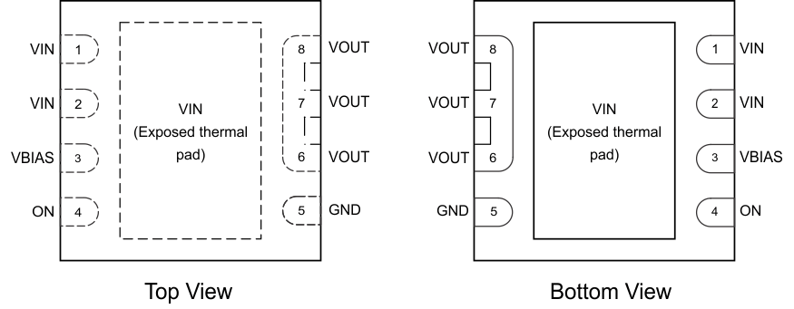
Pin Functions
| PIN | I/O | DESCRIPTION | |
|---|---|---|---|
| NAME | NO. | ||
| VIN | 1, 2 | I | Switch input. Place ceramic bypass capacitor(s) between this pin and GND. See the Detailed Description section for more information. |
| VIN | Exposed thermal Pad | I | Switch input. Place ceramic bypass capacitor(s) between this pin and GND. See the Detailed Description section for more information. |
| VBIAS | 3 | I | Bias voltage. Power supply to the device. |
| ON | 4 | I | Active high switch control input. Do not leave floating. |
| GND | 5 | – | Ground. |
| VOUT | 6, 7, 8 | O | Switch output. Place ceramic bypass capacitor(s) between this pin and GND. See the Detailed Description section for more information. |