ZHCSDK9A March 2015 – April 2015 TPS22953 , TPS22954
PRODUCTION DATA.
- 1 特性
- 2 应用
- 3 说明
- 4 简化电路原理图
- 5 修订历史记录
- 6 Device Comparison Table
- 7 Pin Configuration and Functions
-
8 Specifications
- 8.1 Absolute Maximum Ratings
- 8.2 ESD Ratings
- 8.3 Recommended Operating Conditions
- 8.4 Thermal Information
- 8.5 Electrical Characteristics
- 8.6 Electrical Characteristics, VBIAS = 5 V
- 8.7 Electrical Characteristics, VBIAS = 3.3 V
- 8.8 Electrical Characteristics, VBIAS = 2.5 V
- 8.9 Switching Characteristics, CT = 1000 pF
- 8.10 Switching Characteristics, CT = 0 pF
- 8.11 Typical DC Characteristics
- 8.12 Typical Switching Characteristics
-
9 Detailed Description
- 9.1 Overview
- 9.2 Functional Block Diagram
- 9.3
Feature Description
- 9.3.1 On/Off Control (EN pin)
- 9.3.2 Voltage Monitoring (SNS pin)
- 9.3.3 Power Good (PG Pin)
- 9.3.4 Supervisor Fault Detection and Automatic Restart
- 9.3.5 Manual Restart
- 9.3.6 Thermal Shutdown
- 9.3.7 Quick Output Discharge (QOD) (TPS22954 Only)
- 9.3.8 VIN and VBIAS Voltage Range
- 9.3.9 Adjustable Rise Time (CT pin)
- 9.4 Device Functional Modes
- 10Application and Implementation
- 11Power Supply Recommendations
- 12Layout
- 13器件和文档支持
- 14机械封装和可订购信息
封装选项
机械数据 (封装 | 引脚)
散热焊盘机械数据 (封装 | 引脚)
- DQC|10
订购信息
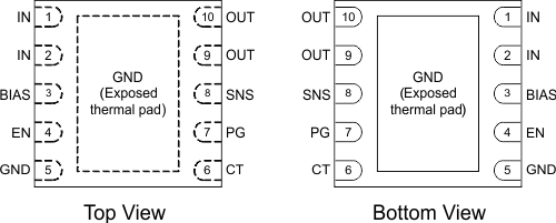
7 Pin Configuration and Functions

Pin Functions
| PIN(1) | I/O | DESCRIPTION | |
|---|---|---|---|
| NAME | NO. | ||
| IN | 1, 2 | I | Switch input. Bypass this input with a ceramic capacitor to GND. |
| BIAS | 3 | I | Bias pin and power supply to the device. |
| EN | 4 | I | Active high switch enable/disable input. Also acts as the input UVLO pin. Use external resistor divider to adjust the UVLO level. Do not leave floating. |
| GND | 5 | – | Device ground. |
| CT | 6 | O | VOUT slew rate control. Place ceramic cap from CT to GND to change the VOUT slew rate of the device and limit the inrush current. CT Capacitor should be rated to 25V or higher. |
| PG | 7 | O | Power good. This pin is open drain which will pull low when the voltage on EN and/or SNS is below their respective VIL level. |
| SNS | 8 | I | Sense pin. Use external resistor divider to adjust the power good level. Do not leave floating. |
| OUT | 9, 10 | O | Switch output. |
| Thermal Pad | – | – | Exposed thermal pad. Tie to GND. |
(1) Pinout applies to all package versions.