ZHCSDK9A March 2015 – April 2015 TPS22953 , TPS22954
PRODUCTION DATA.
- 1 特性
- 2 应用
- 3 说明
- 4 简化电路原理图
- 5 修订历史记录
- 6 Device Comparison Table
- 7 Pin Configuration and Functions
-
8 Specifications
- 8.1 Absolute Maximum Ratings
- 8.2 ESD Ratings
- 8.3 Recommended Operating Conditions
- 8.4 Thermal Information
- 8.5 Electrical Characteristics
- 8.6 Electrical Characteristics, VBIAS = 5 V
- 8.7 Electrical Characteristics, VBIAS = 3.3 V
- 8.8 Electrical Characteristics, VBIAS = 2.5 V
- 8.9 Switching Characteristics, CT = 1000 pF
- 8.10 Switching Characteristics, CT = 0 pF
- 8.11 Typical DC Characteristics
- 8.12 Typical Switching Characteristics
-
9 Detailed Description
- 9.1 Overview
- 9.2 Functional Block Diagram
- 9.3
Feature Description
- 9.3.1 On/Off Control (EN pin)
- 9.3.2 Voltage Monitoring (SNS pin)
- 9.3.3 Power Good (PG Pin)
- 9.3.4 Supervisor Fault Detection and Automatic Restart
- 9.3.5 Manual Restart
- 9.3.6 Thermal Shutdown
- 9.3.7 Quick Output Discharge (QOD) (TPS22954 Only)
- 9.3.8 VIN and VBIAS Voltage Range
- 9.3.9 Adjustable Rise Time (CT pin)
- 9.4 Device Functional Modes
- 10Application and Implementation
- 11Power Supply Recommendations
- 12Layout
- 13器件和文档支持
- 14机械封装和可订购信息
封装选项
机械数据 (封装 | 引脚)
散热焊盘机械数据 (封装 | 引脚)
- DQC|10
订购信息
10 Application and Implementation
NOTE
Information in the following applications sections is not part of the TI component specification, and TI does not warrant its accuracy or completeness. TI’s customers are responsible for determining suitability of components for their purposes. Customers should validate and test their design implementation to confirm system functionality.
10.1 Application Information
This section will highlight some of the design considerations when implementing this device in various applications. A PSPICE model for this device is also available on www.ti.com for further aid.
10.1.1 Input to OutputVoltage Drop
The input to output voltage drop in the device is determined by the RON of the device and the load current. The RON of the device depends upon the VIN and VBIAS conditions of the device. Refer to the RON specification of the device in the Electrical Characteristics table of this datasheet. Once the RON of the device is determined based upon the VIN and VBIAS voltage conditions, use Equation 5 to calculate the input to output voltage drop:

Where:
ΔV = voltage drop from IN to OUT
ILOAD = load current
RON = On-Resistance of the device for a specific VIN and VBIAS
An appropriate ILOAD must be chosen such that the IMAX specification of the device is not violated.
10.1.2 Thermal Considerations
The maximum IC junction temperature should be restricted to just under the thermal shutdown (TSD) limit of the device. To calculate the maximum allowable dissipation, PD(max) for a given output current and ambient temperature, use Equation 6.

Where:
PD(max) = maximum allowable power dissipation
TJ(max) = maximum allowable junction temperature before hitting thermal shutdown (see Electrical Characteristics table)
TA = ambient temperature of the device
θJA = junction to air thermal impedance. See Thermal Information section. This parameter is highly dependent upon board layout.
10.1.3 Automatic Power Sequencing
The PG pin of the TPS22953/54 allows for automatic sequencing of multiple system rails or loads. The accurate SNS voltage monitoring will ensure the first rail is up before the next starts to turn on. This approach provides robust system sequencing and reduces the total inrush current by preventing overlap. The example shows how two rails can be sequenced. There is no limit to the number of rails that can be sequenced in this way
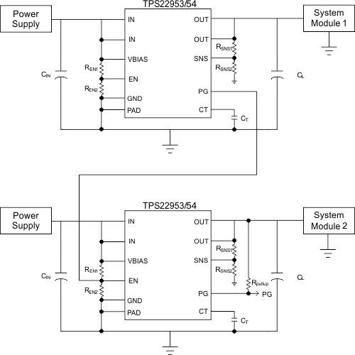 Figure 55. Power Sequencing with PG Control
10.1.4 Monitoring a Downstream Voltage
The SNS pin can be used to monitor other system voltages in addition to VOUT. The status of the monitored voltage will be indicated by the PG pin which can be pulled up to VOUT or another voltage. The figure below shows an example of the TPS22953/54 monitoring the output of a downstream DC/DC regulator. In this case, the switch will turn on when the power supply is above the UVLO, but the PG will not be asserted until the DC/DC regulator has started up.
 Figure 56. Monitoring a Downstream Voltage
In this application, if the DC/DC Regulator is shut down, the supervisor will register this as a fault case and reset the load switch.
10.1.4.1 Monitoring the Input Voltage
The SNS pin can also be used to monitor VIN in the case a MCU GPIO is being used to control the EN. This will allow PG to report on the status of the input voltage when the switch is enabled.
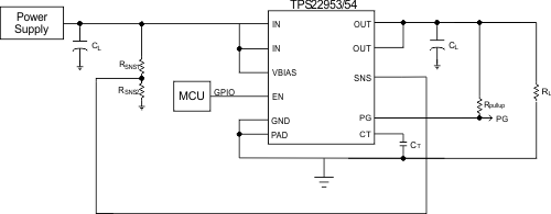 Figure 57. Monitoring Input Voltage
10.2 Typical Application
This application demonstrates how the TPS22953/54 can use used to limit inrush current to output capacitance.
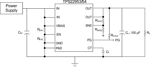 Figure 58. Typical Application Schematic for Powering a Downstream Module
10.2.1 Design Requirements
For this design example, use the following as the input parameters.
Table 1. Design Parameters
| DESIGN PARAMETER | EXAMPLE VALUE |
|---|---|
| VIN | 3.3 V |
| VBIAS | 5.0 V |
| CL | 47 µF |
| Maximum Acceptable Inrush Current | 150mA |
| RL | None |
10.2.2 Detailed Design Procedure
To begin the design process, the designer needs to know the following:
- Input voltage
- BIAS voltage
- Load current
- Load capacitance
- Maximum acceptable inrush current
10.2.2.1 Inrush Current
To determine how much inrush current will be caused by the CL capacitor, use Equation 7:

Where:
IINRUSH = amount of inrush caused by CL
CL = capacitance on VOUT
dt = VOUT Rise Time (typically 10% to 90%)
dVOUT = Change in VOUT Voltage (typically 10% to 90%)
In this case, a Slew Rate slower than 314μs/V will be required to meet the maximum acceptable inrush requirement. Equation 4 can be used to estimate the CT capacitance required for this slew rate.
10.2.3 Application Curves
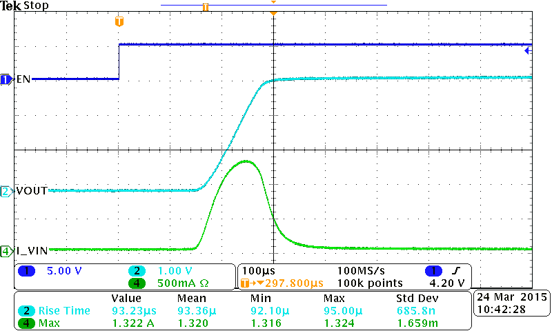
The following Application Curves show the inrush with multiple different CT values. These curves show only a CT capacitance greater than 840pF results in the acceptable inrush current of 150mA.
| CT = 0 pF | ||
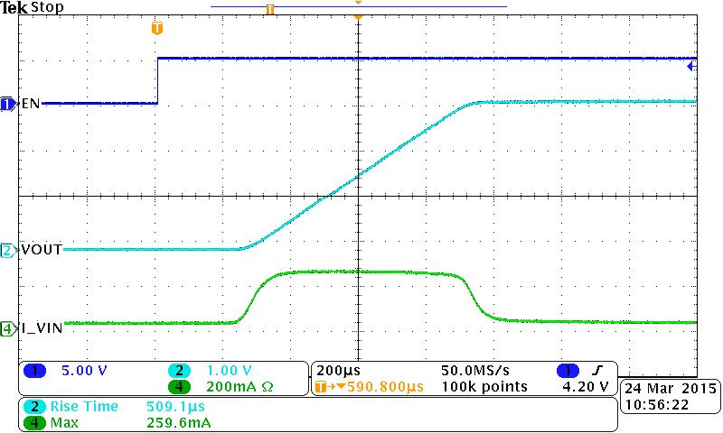
| CT = 470 pF | ||
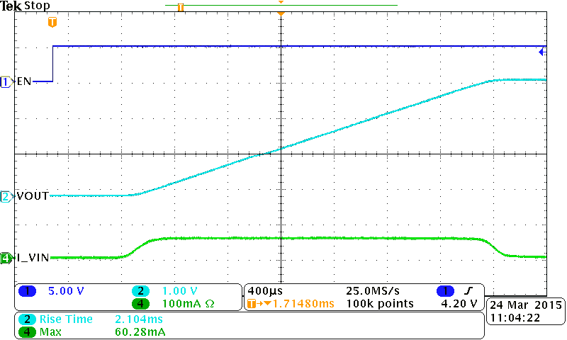
| CT = 2200 pF | ||
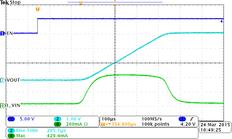
| CT = 220 pF | ||
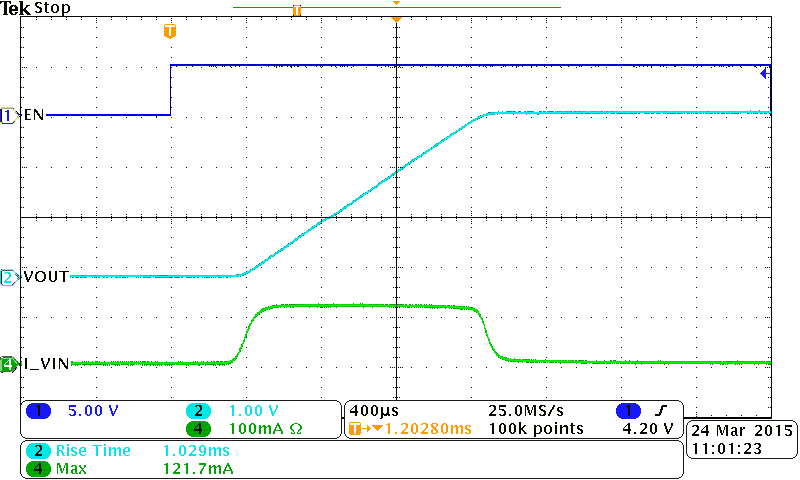
| CT = 1000 pF | ||