ZHCSCE8F April 2014 – May 2019
PRODUCTION DATA.
- 1 特性
- 2 应用
- 3 说明
- 4 修订历史记录
- 5 Device Comparison Table
- 6 Pin Configuration and Functions
-
7 Specifications
- 7.1 Absolute Maximum Ratings
- 7.2 ESD Ratings
- 7.3 Recommended Operating Conditions
- 7.4 Thermal Information
- 7.5 Supply Current Consumption
- 7.6 Electrical Characteristics EN Pin
- 7.7 Thermal Shutdown Feature
- 7.8 Electrical Characteristics nFET Switch
- 7.9 Electrical Characteristics OVP Circuit
- 7.10 Electrical Characteristics VBUS_POWER Circuit
- 7.11 Timing Requirements
- 7.12 TPD1S514-1 Typical Characteristics
-
8 Detailed Description
- 8.1 Overview
- 8.2 Functional Block Diagram
- 8.3
Feature Description
- 8.3.1 Over Voltage Protection on VBUS_CON up to 30 V DC
- 8.3.2 Precision OVP (< ±1% Tolerance)
- 8.3.3 Low RON nFET Switch Supports Host and Charging Mode
- 8.3.4 VBUS_POWER, TPD1S514-1, TPD1S514-2, TPD1S514-3
- 8.3.5 VBUS_POWER, TPD1S514
- 8.3.6 Powering the System When Battery is Discharged
- 8.3.7 ±15 kV IEC 61000-4-2 Level 4 ESD Protection
- 8.3.8 100 V IEC 61000-4-5 µs Surge Protection
- 8.3.9 Startup and OVP Recovery Delay
- 8.3.10 Thermal Shutdown
- 8.4 Device Functional Modes
- 9 Application and Implementation
- 10Power Supply Recommendations
- 11Layout
- 12器件和文档支持
- 13机械、封装和可订购信息
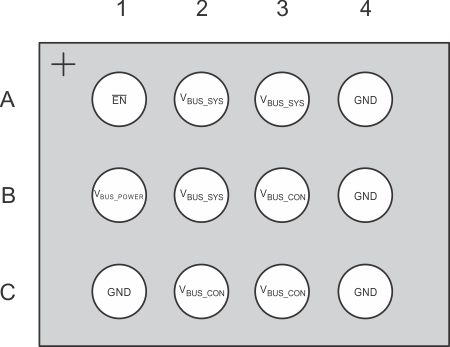
6 Pin Configuration and Functions
YZ Package
12-Pin WCSP
Top Side, See Through View

Pin Functions
| PIN | I/O | DESCRIPTION | |
|---|---|---|---|
| NAME | NO. | ||
| EN | A1 | I | Enable Active-Low Input. Drive EN low to enable the switch. Drive EN high to disable the switch. |
| VBUS_POWER | B1 | O | 5-V Power source controlled by VBUS_CON. |
| VBUS_SYS | A2, A3, B2 | I/O | Connect to internal VBUS plane. |
| VBUS_CON | B3, C2, C3 | I/O | Connect to USB connector VBUS pin; IEC 61000-4-2 ESD protection and IEC 61000-4-5 Surge protection. |
| GND | A4, B4, C1, C4 | G | Connect to PCB ground plane. |