ZHCSCE8F April 2014 – May 2019
PRODUCTION DATA.
- 1 特性
- 2 应用
- 3 说明
- 4 修订历史记录
- 5 Device Comparison Table
- 6 Pin Configuration and Functions
-
7 Specifications
- 7.1 Absolute Maximum Ratings
- 7.2 ESD Ratings
- 7.3 Recommended Operating Conditions
- 7.4 Thermal Information
- 7.5 Supply Current Consumption
- 7.6 Electrical Characteristics EN Pin
- 7.7 Thermal Shutdown Feature
- 7.8 Electrical Characteristics nFET Switch
- 7.9 Electrical Characteristics OVP Circuit
- 7.10 Electrical Characteristics VBUS_POWER Circuit
- 7.11 Timing Requirements
- 7.12 TPD1S514-1 Typical Characteristics
-
8 Detailed Description
- 8.1 Overview
- 8.2 Functional Block Diagram
- 8.3
Feature Description
- 8.3.1 Over Voltage Protection on VBUS_CON up to 30 V DC
- 8.3.2 Precision OVP (< ±1% Tolerance)
- 8.3.3 Low RON nFET Switch Supports Host and Charging Mode
- 8.3.4 VBUS_POWER, TPD1S514-1, TPD1S514-2, TPD1S514-3
- 8.3.5 VBUS_POWER, TPD1S514
- 8.3.6 Powering the System When Battery is Discharged
- 8.3.7 ±15 kV IEC 61000-4-2 Level 4 ESD Protection
- 8.3.8 100 V IEC 61000-4-5 µs Surge Protection
- 8.3.9 Startup and OVP Recovery Delay
- 8.3.10 Thermal Shutdown
- 8.4 Device Functional Modes
- 9 Application and Implementation
- 10Power Supply Recommendations
- 11Layout
- 12器件和文档支持
- 13机械、封装和可订购信息
9.2.1 TPD1S514-1 USB 2.0/3.0 Case 1: Always Enabled
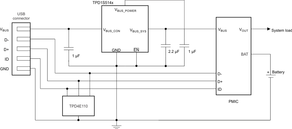
The EN pin can be tied to ground so that the nFET is ON when VUVLO < VBUS_CON < VOVP and an external charger can power VBUS. VBUS_POWER should be tied to ground with a 1-μF capacitor for LDO stability. USB Inrush Current compliance tests will need to be handled by the rest of the system since the start delays tDELAY and tSS implement only after the device changes from disabled to enabled, or after any UVLO or OVP event.
 Figure 10. Always on, TPD1S514-1