ZHCS891G April 2012 – December 2017 TPA3116D2 , TPA3118D2 , TPA3130D2
PRODUCTION DATA.
- 1 特性
- 2 应用
- 3 说明
- 4 修订历史记录
- 5 Pin Configuration and Functions
- 6 Specifications
-
7 Detailed Description
- 7.1 Overview
- 7.2 Functional Block Diagram
- 7.3
Feature Description
- 7.3.1 Gain Setting and Master and Slave
- 7.3.2 Input Impedance
- 7.3.3 Startup and Shutdown Operation
- 7.3.4 PLIMIT Operation
- 7.3.5 GVDD Supply
- 7.3.6 BSPx AND BSNx Capacitors
- 7.3.7 Differential Inputs
- 7.3.8 Device Protection System
- 7.3.9 DC Detect Protection
- 7.3.10 Short-Circuit Protection and Automatic Recovery Feature
- 7.3.11 Thermal Protection
- 7.3.12 Device Modulation Scheme
- 7.3.13 Efficiency: LC Filter Required with the Traditional Class-D Modulation Scheme
- 7.3.14 Ferrite Bead Filter Considerations
- 7.3.15 When to Use an Output Filter for EMI Suppression
- 7.3.16 AM Avoidance EMI Reduction
- 7.4 Device Functional Modes
- 8 Application and Implementation
- 9 Power Supply Recommendations
- 10Layout
- 11器件和文档支持
- 12机械、封装和可订购信息
7.3.12.2 MODSEL = HIGH: 1SPW-modulation
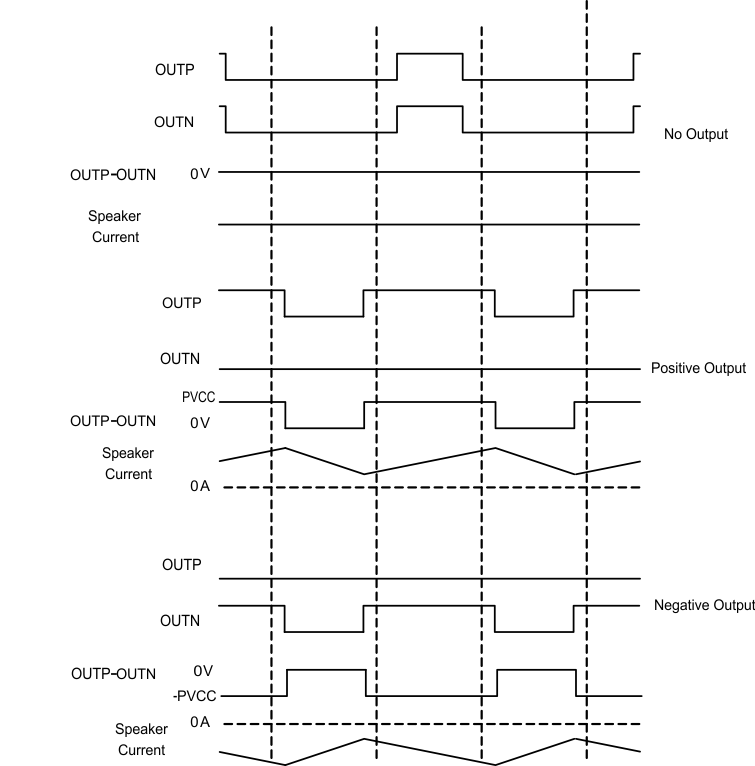
The 1SPW mode alters the normal modulation scheme in order to achieve higher efficiency with a slight penalty in THD degradation and more attention required in the output filter selection. In 1SPW mode the outputs operate at ~15% modulation during idle conditions. When an audio signal is applied one output will decrease and one will increase. The decreasing output signal will quickly rail to GND at which point all the audio modulation takes place through the rising output. The result is that only one output is switching during a majority of the audio cycle. Efficiency is improved in this mode due to the reduction of switching losses. The THD penalty in 1SPW mode is minimized by the high performance feedback loop. The resulting audio signal at each half output has a discontinuity each time the output rails to GND. This can cause ringing in the audio reconstruction filter unless care is taken in the selection of the filter components and type of filter used.
 Figure 33. 1SPW Mode Modulation