ZHCS891G April 2012 – December 2017 TPA3116D2 , TPA3118D2 , TPA3130D2
PRODUCTION DATA.
- 1 特性
- 2 应用
- 3 说明
- 4 修订历史记录
- 5 Pin Configuration and Functions
- 6 Specifications
-
7 Detailed Description
- 7.1 Overview
- 7.2 Functional Block Diagram
- 7.3
Feature Description
- 7.3.1 Gain Setting and Master and Slave
- 7.3.2 Input Impedance
- 7.3.3 Startup and Shutdown Operation
- 7.3.4 PLIMIT Operation
- 7.3.5 GVDD Supply
- 7.3.6 BSPx AND BSNx Capacitors
- 7.3.7 Differential Inputs
- 7.3.8 Device Protection System
- 7.3.9 DC Detect Protection
- 7.3.10 Short-Circuit Protection and Automatic Recovery Feature
- 7.3.11 Thermal Protection
- 7.3.12 Device Modulation Scheme
- 7.3.13 Efficiency: LC Filter Required with the Traditional Class-D Modulation Scheme
- 7.3.14 Ferrite Bead Filter Considerations
- 7.3.15 When to Use an Output Filter for EMI Suppression
- 7.3.16 AM Avoidance EMI Reduction
- 7.4 Device Functional Modes
- 8 Application and Implementation
- 9 Power Supply Recommendations
- 10Layout
- 11器件和文档支持
- 12机械、封装和可订购信息
7.3.10 Short-Circuit Protection and Automatic Recovery Feature
The TPA31xxD2 family has protection from over current conditions caused by a short circuit on the output stage. The short circuit protection fault is reported on the FAULTZ pin as a low state. The amplifier outputs are switched to a high impedance state when the short circuit protection latch is engaged. The latch can be cleared by cycling the SDZ pin through the low state.
If automatic recovery from the short circuit protection latch is desired, connect the FAULTZ pin directly to the SDZ pin. This allows the FAULTZ pin function to automatically drive the SDZ pin low which clears the short-circuit protection latch.
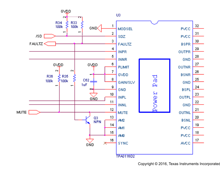
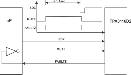
In systems where a possibility of a permanent short from the output to PVDD or to a high voltage battery like a car battery can occur, pull the MUTE pin low with the FAULTZ signal with a inverting transistor to ensure a high-Z restart, like shown in the figure below:
 Figure 30. MUTE Driven by Inverted FAULTZ
 Figure 31. Timing Requirement for SDZ