ZHCS891G April 2012 – December 2017 TPA3116D2 , TPA3118D2 , TPA3130D2
PRODUCTION DATA.
- 1 特性
- 2 应用
- 3 说明
- 4 修订历史记录
- 5 Pin Configuration and Functions
- 6 Specifications
-
7 Detailed Description
- 7.1 Overview
- 7.2 Functional Block Diagram
- 7.3
Feature Description
- 7.3.1 Gain Setting and Master and Slave
- 7.3.2 Input Impedance
- 7.3.3 Startup and Shutdown Operation
- 7.3.4 PLIMIT Operation
- 7.3.5 GVDD Supply
- 7.3.6 BSPx AND BSNx Capacitors
- 7.3.7 Differential Inputs
- 7.3.8 Device Protection System
- 7.3.9 DC Detect Protection
- 7.3.10 Short-Circuit Protection and Automatic Recovery Feature
- 7.3.11 Thermal Protection
- 7.3.12 Device Modulation Scheme
- 7.3.13 Efficiency: LC Filter Required with the Traditional Class-D Modulation Scheme
- 7.3.14 Ferrite Bead Filter Considerations
- 7.3.15 When to Use an Output Filter for EMI Suppression
- 7.3.16 AM Avoidance EMI Reduction
- 7.4 Device Functional Modes
- 8 Application and Implementation
- 9 Power Supply Recommendations
- 10Layout
- 11器件和文档支持
- 12机械、封装和可订购信息
6.7 Typical Characteristics
fs = 400 kHz, BD Mode (unless otherwise noted)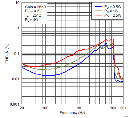 Figure 1. Total Harmonic Distortion + Noise (BTL) vs Frequency
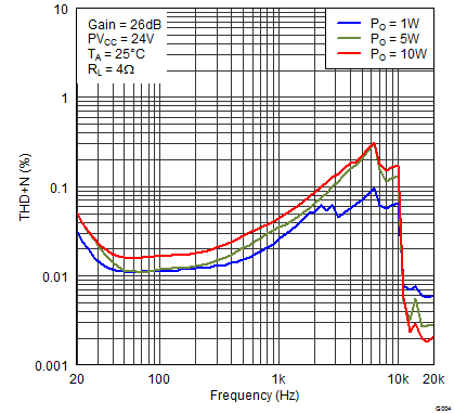 Figure 3. Total Harmonic Distortion + Noise (BTL) vs Frequency
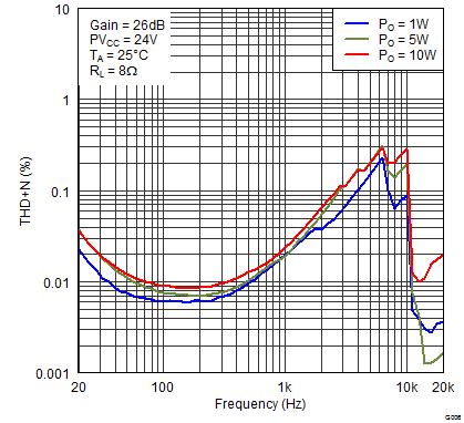 Figure 5. Total Harmonic Distortion + Noise (BTL) vs Frequency
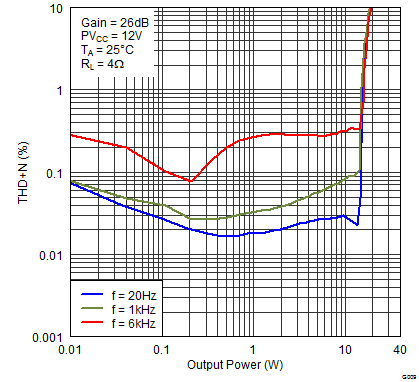 Figure 7. Total Harmonic Distortion + Noise (BTL) vs Output Power
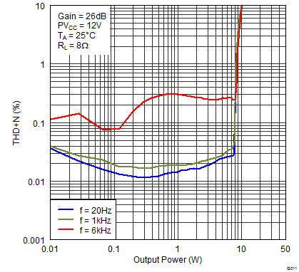 Figure 9. Total Harmonic Distortion + Noise (BTL) vs Output Power
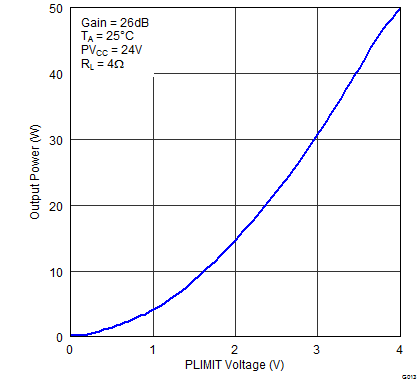 Figure 11. Output Power (BTL) vs Plimit Voltage
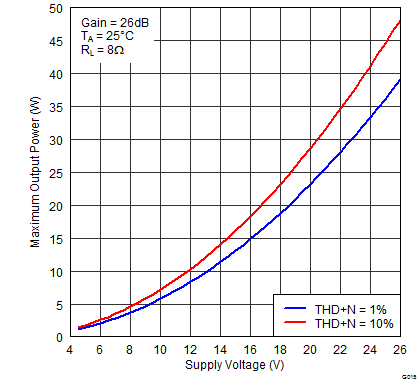 Figure 13. Maximum Output Power (BTL) vs Supply Voltage
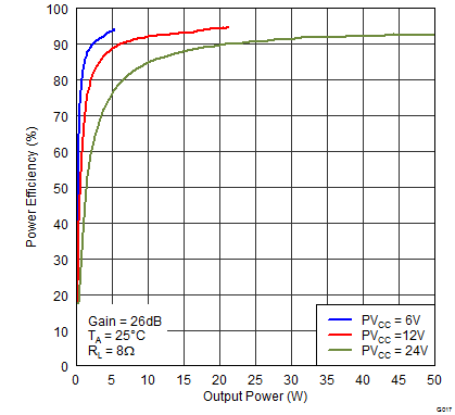 Figure 15. Power Efficiency (BTL) vs Output Power
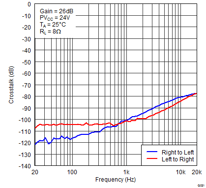 Figure 17. Crosstalk vs Frequency
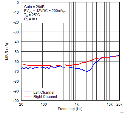 Figure 19. Supply Ripple Rejection Ratio (BTL) vs Frequency
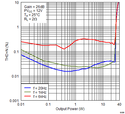 Figure 21. Total Harmonic Distortion + Noise (PBTL) vs Output Power
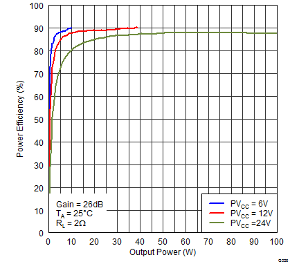 Figure 23. Power Efficiency (PBTL) vs Output Power
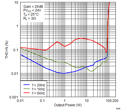 Figure 25. Total Harmonic Distortion + Noise (PBTL) vs Output Power
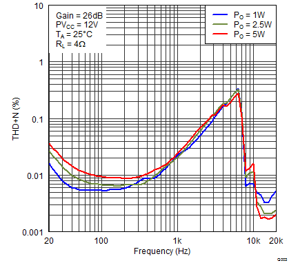 Figure 2. Total Harmonic Distortion + Noise (BTL) vs Frequency
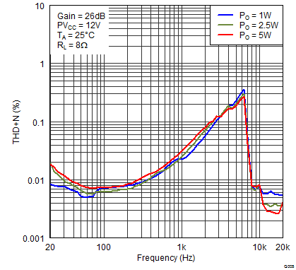 Figure 4. Total Harmonic Distortion + Noise (BTL) vs Frequency
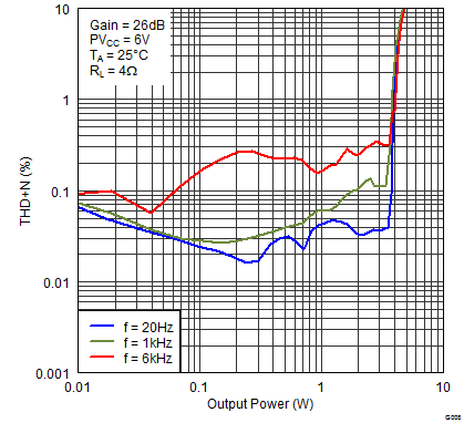 Figure 6. Total Harmonic Distortion + Noise (BTL) vs Output Power
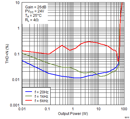 Figure 8. Total Harmonic Distortion + Noise (BTL) vs Output Power
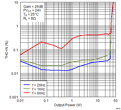 Figure 10. Total Harmonic Distortion + Noise (BTL) vs Output Power
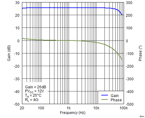 Figure 12. Gain/Phase (BTL) vs Frequency
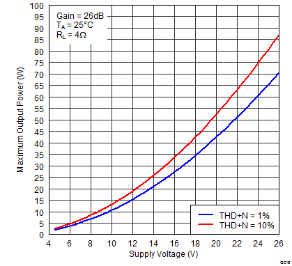 Figure 14. Maximum Output Power (BTL) vs Supply Voltage
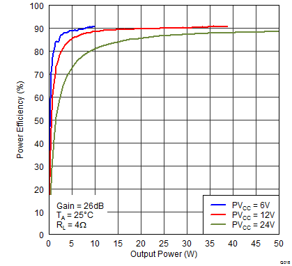 Figure 16. Power Efficiency (BTL) vs Output Power
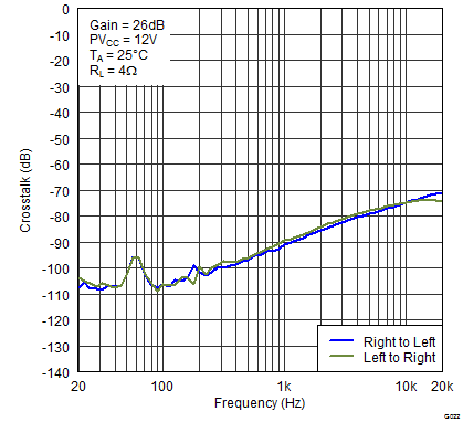 Figure 18. Crosstalk vs Frequency
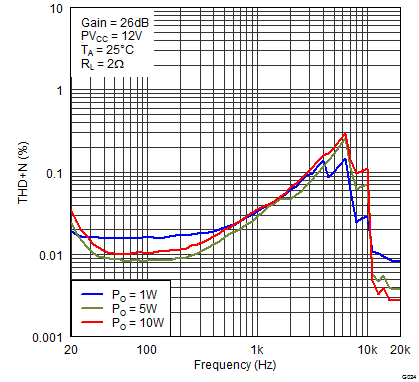 Figure 20. Total Harmonic Distortion + Noise (PBTL) vs Frequency
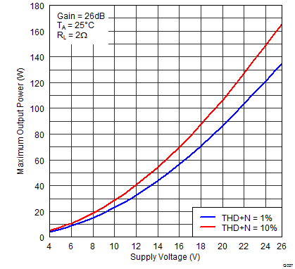 Figure 22. Maximum Output Power (PBTL) vs Supply Voltage
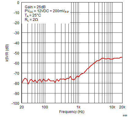 Figure 24. Supply Ripple Rejection Ratio (PBTL) vs Frequency
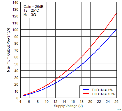 Figure 26. Maximum Output Power (PBTL) vs Supply Voltage