ZHCSKF7A May   2019  – January 2023 TAS5825P

PRODUCTION DATA  

  1. 特性
  2. 应用
  3. 说明
  4. Revision History
  5. Device Comparison Table
  6. Pin Configuration and Functions
  7. Specifications
    1. 7.1 Absolute Maximum Ratings
    2. 7.2 ESD Ratings
    3. 7.3 Recommended Operating Conditions
    4. 7.4 Thermal Information
    5. 7.5 Electrical Characteristics
    6. 7.6 Timing Requirements
    7. 7.7 Typical Characteristics
      1. 7.7.1 Bridge Tied Load (BTL) Configuration Curves with Hybrid Modulation
      2. 7.7.2 Parallel Bridge Tied Load (PBTL) Configuration With Hybrid Modulation
      3. 7.7.3 Bridge Tied Load (BTL) Configuration Curves with BD Modulation
      4. 7.7.4 Parallel Bridge Tied Load (PBTL) Configuration With BD Modulation
  8. Parameter Measurement Information
  9. Detailed Description
    1. 9.1 Overview
    2. 9.2 Functional Block Diagram
    3. 9.3 Feature Description
      1. 9.3.1 Power Supplies
      2. 9.3.2 Device Clocking
      3. 9.3.3 Serial Audio Port – Clock Rates
      4. 9.3.4 Clock Halt Auto-Recovery
      5. 9.3.5 Sample Rate on the Fly Change
      6. 9.3.6 Serial Audio Port - Data Formats and Bit Depths
      7. 9.3.7 Digital Audio Processing
      8. 9.3.8 Class-D Audio Amplifier
        1. 9.3.8.1 Speaker Amplifier Gain Select
        2. 9.3.8.2 Class D Loop Bandwidth and Switching Frequency Setting
    4. 9.4 Device Functional Modes
      1. 9.4.1 Software Control
      2. 9.4.2 Speaker Amplifier Operating Modes
        1. 9.4.2.1 BTL Mode
        2. 9.4.2.2 PBTL Mode
      3. 9.4.3 Low EMI Modes
        1. 9.4.3.1 Spread Spectrum
        2. 9.4.3.2 Channel to Channel Phase Shift
        3. 9.4.3.3 Multi-Devices PWM Phase Synchronization
          1. 9.4.3.3.1 Phase Synchronization With I2S Clock In Startup Phase
          2. 9.4.3.3.2 Phase Synchronization With GPIO
      4. 9.4.4 Thermal Foldback
      5. 9.4.5 Device State Control
      6. 9.4.6 Device Modulation
        1. 9.4.6.1 BD Modulation
        2. 9.4.6.2 1SPW Modulation
        3. 9.4.6.3 Hybrid Modulation
    5. 9.5 Programming and Control
      1. 9.5.1 I2 C Serial Communication Bus
      2. 9.5.2 I2 C Peripheral Address
        1. 9.5.2.1 Random Write
        2. 9.5.2.2 Sequential Write
        3. 9.5.2.3 Random Read
        4. 9.5.2.4 Sequential Read
        5. 9.5.2.5 DSP Memory Book, Page and BQ update
        6. 9.5.2.6 Checksum
          1. 9.5.2.6.1 Cyclic Redundancy Check (CRC) Checksum
          2. 9.5.2.6.2 Exclusive or (XOR) Checksum
      3. 9.5.3 Control via Software
        1. 9.5.3.1 Startup Procedures
        2. 9.5.3.2 Shutdown Procedures
        3. 9.5.3.3 Protection and Monitoring
          1. 9.5.3.3.1 Overcurrent Limit (Cycle-By-Cycle)
          2. 9.5.3.3.2 Overcurrent Shutdown (OCSD)
          3. 9.5.3.3.3 DC Detect
    6. 9.6 Register Maps
      1. 9.6.1 CONTROL PORT Registers
  10. 10Application and Implementation
    1. 10.1 Application Information
      1. 10.1.1 Bootstrap Capacitors
      2. 10.1.2 Inductor Selections
      3. 10.1.3 Power Supply Decoupling
      4. 10.1.4 Output EMI Filtering
    2. 10.2 Typical Applications
      1. 10.2.1 2.0 (Stereo BTL) System
      2. 10.2.2 79
      3. 10.2.3 Design Requirements
      4. 10.2.4 Detailed Design procedures
        1. 10.2.4.1 Step One: Hardware Integration
        2. 10.2.4.2 Step Two: Hardware Integration
        3. 10.2.4.3 Step Three: Software Integration
      5. 10.2.5 Application Curves
      6. 10.2.6 MONO (PBTL) Systems
      7. 10.2.7 Application Curves
    3. 10.3 Power Supply Recommendations
      1. 10.3.1 DVDD Supply
      2. 10.3.2 PVDD Supply
    4. 10.4 Layout
      1. 10.4.1 Layout Guidelines
        1. 10.4.1.1 General Guidelines for Audio Amplifiers
        2. 10.4.1.2 Importance of PVDD Bypass Capacitor Placement on PVDD Network
        3. 10.4.1.3 Optimizing Thermal Performance
          1. 10.4.1.3.1 Device, Copper, and Component Layout
          2. 10.4.1.3.2 Stencil Pattern
            1. 10.4.1.3.2.1 PCB footprint and Via Arrangement
            2. 10.4.1.3.2.2 Solder Stencil
      2. 10.4.2 Layout Example
  11. 11Device and Documentation Support
    1. 11.1 Device Support
      1. 11.1.1 Device Nomenclature
      2. 11.1.2 Development Support
    2. 11.2 Receiving Notification of Documentation Updates
    3. 11.3 支持资源
    4. 11.4 Trademarks
    5. 11.5 静电放电警告
    6. 11.6 术语表
  12. 12Mechanical, Packaging, and Orderable Information

封装选项

机械数据 (封装 | 引脚)
散热焊盘机械数据 (封装 | 引脚)
订购信息

说明

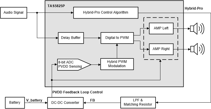
TAS5825P 是一款采用先进 Hybrid-Pro 算法的立体声高效闭环音频 D 类音频放大器,可提高系统效率并减少发热而不会产生削波失真。

音频放大器的电源电压 (PVDD) 通常由直流/直流转换器提供。与固定 PVDD 相比,基于音频信号而波动的可变 PVDD 可显著提高效率,降低空闲电流并减少发热。

TAS5825P 的强大音频 DSP 内核实现了一种称为 Hybrid-Pro 的专有算法。Hybrid-Pro 算法可检测即将发生的音频功率需求,并通过 Hybrid-Pro 反馈引脚 (HPFB) 为前直流/直流转换器提供 PWM 控制信号。TAS5825P 支持高达 4ms 的延迟缓冲器,以提前查看音频信号并防止音频削波失真。在各种实验中,TAS5825P 在连续播放音乐时可将 1S 和 2S 电池的运行时间延长 50% 以上。

器件信息(1)
器件型号封装封装尺寸(标称值)
TAS5825PVQFN (32) RHB5.00mm × 5.00mm
如需了解所有可用封装,请参阅数据表末尾的可订购产品附录。
GUID-A1A7D99F-8D5B-4AA7-AB10-720D6E772796-low.gif