ZHCSFW6A December 2016 – February 2020 SN65MLVD206B
PRODUCTION DATA.
- 1 特性
- 2 应用
- 3 说明
- 4 修订历史记录
- 5 Pin Configuration and Functions
-
6 Specifications
- Table 1. Absolute Maximum Ratings
- Table 2. ESD Ratings
- Table 3. Recommended Operating Conditions
- Table 4. Thermal Information
- Table 5. Electrical Characteristics
- Table 6. Electrical Characteristics – Driver
- Table 7. Electrical Characteristics – Receiver
- Table 8. Electrical Characteristics – BUS Input and Output
- Table 9. Switching Characteristics – Driver
- Table 10. Switching Characteristics – Receiver
- 6.1 Typical Characteristics
- 7 Parameter Measurement Information
- 8 Detailed Description
-
9 Application and Implementation
- 9.1 Application Information
- 9.2
Typical Application
- 9.2.1 Multipoint Communications
- 9.2.2 Design Requirements
- 9.2.3
Detailed Design Procedure
- 9.2.3.1 Supply Voltage
- 9.2.3.2 Supply Bypass Capacitance
- 9.2.3.3 Driver Input Voltage
- 9.2.3.4 Driver Output Voltage
- 9.2.3.5 Termination Resistors
- 9.2.3.6 Receiver Input Signal
- 9.2.3.7 Receiver Input Threshold (Failsafe)
- 9.2.3.8 Receiver Output Signal
- 9.2.3.9 Interconnecting Media
- 9.2.3.10 PCB Transmission Lines
- 9.2.4 Application Curves
- 10Power Supply Recommendations
- 11Layout
- 12器件和文档支持
- 13机械、封装和可订购信息
11.1.1 Microstrip vs. Stripline Topologies
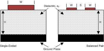
As per SLLD009, printed-circuit boards usually offer designers two transmission line options: Microstrip and stripline. Microstrips are traces on the outer layer of a PCB, as shown in Figure 22.
 Figure 22. Microstrip Topology
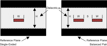
 On the other hand, striplines are traces between two ground planes. Striplines are less prone to emissions and susceptibility problems because the reference planes effectively shield the embedded traces. However, from the standpoint of high-speed transmission, juxtaposing two planes creates additional capacitance. TI recommends routing M-LVDS signals on microstrip transmission lines if possible. The PCB traces allow designers to specify the necessary tolerances for ZO based on the overall noise budget and reflection allowances. Footnotes 1(1), 2(2), and 3(3) provide formulas for ZO and tPD for differential and single-ended traces. (1)(2)(3)
 Figure 23. Stripline Topology