ZHCSN67N July   1997  – April 2021 SN55LVDS31 , SN65LVDS31 , SN65LVDS3487 , SN65LVDS9638

PRODUCTION DATA  

  1. 特性
  2. 应用
  3. 说明
  4. Revision History
  5. 说明(续)
  6. Pin Configuration and Functions
  7. Specifications
    1. 7.1 Absolute Maximum Ratings (1)
    2. 7.2 ESD Ratings
    3. 7.3 Recommended Operating Conditions
    4. 7.4 Thermal Information
    5. 7.5 Electrical Characteristics: SN55LVDS31
    6. 7.6 Electrical Characteristics: SN65LVDSxxxx
    7. 7.7 Switching Characteristics: SN55LVDS31
    8. 7.8 Switching Characteristics: SN65LVDSxxxx
    9. 7.9 Typical Characteristics
      1. 7.9.1 17
  8. Parameter Measurement Information
    1. 8.1 19
  9. Detailed Description
    1. 9.1 Overview
    2. 9.2 Functional Block Diagram
    3. 9.3 Feature Description
      1. 9.3.1 Driver Disabled Output
      2. 9.3.2 NC Pins
      3. 9.3.3 Unused Enable Pins
      4. 9.3.4 Driver Equivalent Schematics
    4. 9.4 Device Functional Modes
  10. 10Application and Implementation
    1. 10.1 Application Information
    2. 10.2 Typical Application
      1. 10.2.1 Point-to-Point Communications
        1. 10.2.1.1 Design Requirements
        2. 10.2.1.2 Detailed Design Procedure
          1. 10.2.1.2.1 Driver Supply Voltage
          2. 10.2.1.2.2 Driver Bypass Capacitance
          3. 10.2.1.2.3 Driver Output Voltage
          4. 10.2.1.2.4 Interconnecting Media
          5. 10.2.1.2.5 PCB Transmission Lines
          6. 10.2.1.2.6 Termination Resistor
          7. 10.2.1.2.7 Driver NC Pins
        3. 10.2.1.3 Application Curve
      2. 10.2.2 Multidrop Communications
        1. 10.2.2.1 Design Requirements
        2. 10.2.2.2 Detailed Design Procedure
          1. 10.2.2.2.1 Interconnecting Media
        3. 10.2.2.3 Application Curve
  11. 11Power Supply Recommendations
    1. 11.1 49
  12. 12Layout
    1. 12.1 Layout Guidelines
      1. 12.1.1 Microstrip vs. Stripline Topologies
      2. 12.1.2 Dielectric Type and Board Construction
      3. 12.1.3 Recommended Stack Layout
      4. 12.1.4 Separation Between Traces
      5. 12.1.5 Crosstalk and Ground Bounce Minimization
    2. 12.2 Layout Example
  13. 13Device and Documentation Support
    1. 13.1 Device Support
      1. 13.1.1 Other LVDS Products
    2. 13.2 Documentation Support
      1. 13.2.1 Related Information
      2. 13.2.2 接收文档更新通知
      3. 13.2.3 Related Links
    3. 13.3 支持资源
    4. 13.4 Trademarks
    5. 13.5 静电放电警告
    6. 13.6 术语表
  14. 14Mechanical, Packaging, and Orderable Information

封装选项

请参考 PDF 数据表获取器件具体的封装图。

机械数据 (封装 | 引脚)
  • PW|16
  • NS|16
  • D|16
散热焊盘机械数据 (封装 | 引脚)
订购信息

Application Information

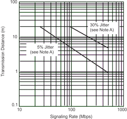
The SNx5LVDSxx devices are dual- and quad-channel LVDS drivers. These devices are generally used as building blocks for high-speed, point-to-point, data transmission where ground differences are less than 1 V. LVDS drivers and receivers provide high-speed signaling rates that are often implemented with ECL class devices without the ECL power and dual-supply requirements. A common question with any class of driver is how far and how fast can the devices operate. While individual drivers and receivers have specifications that define their inherent switching rate, a communication link will quite often be limited by the impairments introduced by the interconnecting media. #SLLS2618289 shows the typical relationship between signaling rate and distance achievable depends on the quality of the eye pattern at the receiver that is either desired or needed. #SLLS2618289 shows the curves representing 5% and 30% eye closure due to inter-symbol interference (ISI).
GUID-7F0C236D-BEF0-437D-9D59-D8BC6322A936-low.gif
24 A WG UTP 96 Ω (PVC Dielectric)
This parameter is the percentage of distortion of the unit interval (UI) with a pseudorandom data pattern.
Figure 10-1 Typical Transmission Distance vs Signaling Rate