ZHCSN67N July 1997 – April 2021 SN55LVDS31 , SN65LVDS31 , SN65LVDS3487 , SN65LVDS9638
PRODUCTION DATA
- 1 特性
- 2 应用
- 3 说明
- 4 Revision History
- 5 说明(续)
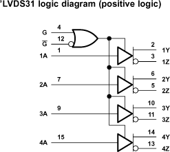
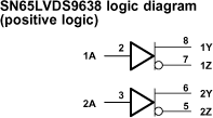
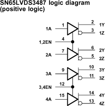
- 6 Pin Configuration and Functions
-
7 Specifications
- 7.1 Absolute Maximum Ratings (1)
- 7.2 ESD Ratings
- 7.3 Recommended Operating Conditions
- 7.4 Thermal Information
- 7.5 Electrical Characteristics: SN55LVDS31
- 7.6 Electrical Characteristics: SN65LVDSxxxx
- 7.7 Switching Characteristics: SN55LVDS31
- 7.8 Switching Characteristics: SN65LVDSxxxx
- 7.9 Typical Characteristics
- 8 Parameter Measurement Information
- 9 Detailed Description
- 10Application and Implementation
- 11Power Supply Recommendations
- 12Layout
- 13Device and Documentation Support
- 14Mechanical, Packaging, and Orderable Information
封装选项
请参考 PDF 数据表获取器件具体的封装图。
机械数据 (封装 | 引脚)
- PW|16
- NS|16
- D|16
散热焊盘机械数据 (封装 | 引脚)
- D|16
订购信息
9.2 Functional Block Diagram