ZHCSFG5A September 2016 – November 2016 SN65HVD233-Q1 , SN65HVD234-Q1 , SN65HVD235-Q1
PRODUCTION DATA.
- 1 特性
- 2 应用
- 3 说明
- 4 修订历史记录
- 5 说明 (续)
- 6 Device Comparison Table
- 7 Pin Configuration and Functions
-
8 Specifications
- 8.1 Absolute Maximum Ratings
- 8.2 ESD Ratings
- 8.3 Recommended Operating Conditions
- 8.4 Thermal Information
- 8.5 Electrical Characteristics: Driver
- 8.6 Electrical Characteristics: Receiver
- 8.7 Switching Characteristics: Driver
- 8.8 Switching Characteristics: Receiver
- 8.9 Switching Characteristics: Device
- 8.10 Typical Characteristics
- 9 Parameter Measurement Information
- 10Detailed Description
- 11Application and Implementation
- 12Power Supply Recommendations
- 13Layout
- 14器件和文档支持
- 15机械、封装和可订购信息
10 Detailed Description
10.1 Overview
This family of CAN transceivers is compatible with the ISO 11898-2 high-speed controller-area-network (CAN) physical layer standard. These devices are designed to interface between the differential bus lines in CAN and the CAN protocol controller at data rates up to 1 Mpbs.
10.2 Functional Block Diagrams
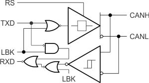
 Figure 29. SN65HVD233-Q1 Functional Block Diagram
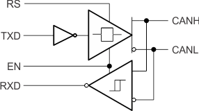
 Figure 30. SN65HVD234-Q1 Functional Block Diagram
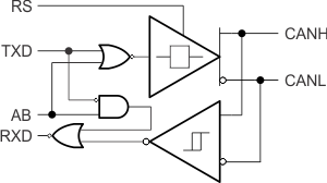
 Figure 31. SN65HVD235-Q1 Functional Block Diagram
10.3 Feature Description
10.3.1 Diagnostic Loopback (SN65HVD233-Q1)
The diagnostic loopback or internal loopback function of the SN65HVD233-Q1 device is enabled with a high-level input on pin 5, LBK. This mode disables the driver output while keeping the bus pins biased to the recessive state. This mode also redirects the TXD data input (transmit data) through logic to the received data output pin, thus creating an internal loopback of the transmit-to-receive data path. This mimics the loopback that occurs normally with a CAN transceiver, because the receiver loops back the driven output to the RXD (receive data) pin. This mode allows the host protocol controller to input and read back a bit sequence or CAN messages to perform diagnostic routines without disturbing the CAN bus. A typical CAN bus application is displayed in Figure 37.
If the LBK pin is not used, it may be tied to ground (GND). However, it is pulled low internally (defaults to a low-level input) and may be left open if not in use.
10.3.2 Autobaud Loopback (SN65HVD235-Q1)
The autobaud loopback mode of the SN65HVD235-Q1 device is enabled by placing a high-level input on pin 5, AB. In autobaud mode, the driver output is disabled, thus blocking the TXD pin-to-bus path and the bus transmit function of the transceiver. The bus pins remain biased to recessive. The receiver-to-RXD pin path of the device remains operational, allowing bus activity to be monitored. In addition, the autobaud mode includes an internal logic loopback path from the TXD pin to the RXD pin so the local node can transmit to itself in sync with bus traffic while not disturbing messages on the bus. Thus if the CAN controller of the local node generates an error frame, it is not transmitted to the bus, but is detected only by the local CAN controller. This is especially helpful to determine if the local node is set to the same baud rate as the network, and if not, to adjust it to the network baud rate (autobaud detection).
Autobaud detection is best suited to applications that have a known selection of baud rates. For example, if an application has optional settings of 125 kbps, 250 kbps, or 500 kbps. Once the SN65HVD235-Q1 device is placed into autobaud loopback mode, the application software could assume the first baud rate of 125 kbps. It then waits for a message to be transmitted by another node on the bus. If the wrong baud rate has been selected, an error message is generated by the local CAN controller because the sample times will not be at the correct time. However, because the bus-transmit function of the device has been disabled, no other nodes receive the error frame generated by the local CAN controller of this node.
The application would then make use of the status register indications of the local CAN controller for message-received and error-warning status to determine if the set baud rate is correct or not. The warning status indicates that the CAN controller error counters have been incremented. A message received status indicates that a good message has been received. If an error is generated, the application then sets the CAN controller to the next possibly valid baud rate, and waits to receive another message. This pattern is repeated until an error-free message has been received, thus the correct baud rate has been selected. At this point, the application places the SN65HVD235-Q1 device in a normal transmitting mode by setting pin 5 to a low level, thus enabling bus-transmit and bus-receive functions to normal operating states for the transceiver.
If the AB pin is not used, it may be tied to ground (GND). However, it is pulled low internally (defaults to a low-level input) and may be left open if not in use.
10.3.3 Slope Control
The rise and fall slope of the SN65HVD233-Q1, SN65HVD234-Q1, and SN65HVD235-Q1 driver output can be adjusted by connecting a resistor from RS (pin 8) to ground (GND) as shown in Figure 32, or to a low level input voltage as shown in Figure 33.
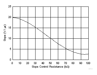
The slope of the driver output signal is proportional to the output current of the pin. This slope control is implemented with an external resistor value of 10 kΩ to achieve an approximately 15-V/µs slew rate, and up to 100 kΩ to achieve an approximately 2-V/μs slew rate. A typical slew-rate versus pulldown-resistance graph is shown in Figure 34. Typical driver output waveforms with slope control are displayed in Figure 40.
 Figure 32. Ground Connection for Selecting Slope-Control or Standby Mode
 Figure 33. DSP Connection for Selecting Slope-Control or Standby Mode
 Figure 34. SN65HVD233-Q1 Driver Output-Signal Slope vs Slope-Control Resistance Value
10.3.4 Standby
If a high-level input (> 0.75 VCC) is applied to RS (pin 8), the circuit enters a low-current, listen only standby mode during which the driver is switched off and the receiver remains active. If using this mode to save system power while waiting for bus traffic, the local controller can monitor the RXD output pin for a falling edge which indicates that a dominant signal was driven onto the CAN bus. The local controller can then drive the RS pin low to return to slope-control mode or high-speed mode.
10.3.5 Thermal Shutdown
If the junction temperature of the device exceeds the thermal shutdown threshold, the device turns off the CAN driver circuits, thus blocking the TXD pin-to-bus transmission path. The shutdown condition is cleared when the junction temperature drops sufficiently below the thermal shutdown temperature of the device. The CAN bus pins are high-impedance and biased to the recessive level during a thermal shutdown, and the receiver-to-RXD pin path remains operational.
10.4 Device Functional Modes
Table 2. Driver (SN65HVD233-Q1 or SN65HVD235-Q1)
| INPUTS | OUTPUTS | ||||
|---|---|---|---|---|---|
| TXD | LBK or AB | RS | CANH | CANL | BUS STATE |
| X | X | > 0.75 VCC | Z | Z | Recessive |
| L | L or open | ≤ 0.33 VCC | H | L | Dominant |
| H or open | X | Z | Z | Recessive | |
| X | H | ≤ 0.33 VCC | Z | Z | Recessive |
Table 3. Driver (SN65HVD234-Q1)
| INPUTS | OUTPUTS | ||||
|---|---|---|---|---|---|
| TXD | EN | RS | CANH | CANL | BUS STATE |
| L | H | ≤ 0.33 VCC | H | L | Dominant |
| H | X | ≤ 0.33 VCC | Z | Z | Recessive |
| Open | X | X | Z | Z | Recessive |
| X | X | > 0.75 VCC | Z | Z | Recessive |
| X | L or open | X | Z | Z | Recessive |
Table 4. Receiver (SN65HVD233-Q1)(1)
| INPUTS | OUTPUT | |||
|---|---|---|---|---|
| BUS STATE | VID = V(CANH) – V(CANL) | LBK | TXD | RXD |
| Dominant | VID ≥ 0.9 V | L or open | X | L |
| Recessive | VID ≤ 0.5 V or open | L or open | H or open | H |
| ? | 0.5 V < VID < 0.9 V | L or open | H or open | ? |
| X | X | H | L | L |
| X | X | H | H | H |
Table 5. Receiver (SN65HVD235-Q1)(1)
| INPUTS | OUTPUT | |||
|---|---|---|---|---|
| BUS STATE | VID = V(CANH)–V(CANL) | AB | TXD | RXD |
| Dominant | VID ≥ 0.9 V | L or open | X | L |
| Recessive | VID ≤ 0.5 V or open | L or open | H or open | H |
| ? | 0.5 V < VID <0.9 V | L or open | H or open | ? |
| Dominant | VID ≥ 0.9 V | H | X | L |
| Recessive | VID ≤ 0.5 V or open | H | H | H |
| Recessive | VID ≤ 0.5 V or open | H | L | L |
| ? | 0.5 V < VID <0.9 V | H | L | L |
Table 6. Receiver (SN65HVD234-Q1)(1)
| INPUTS | OUTPUT | ||
|---|---|---|---|
| BUS STATE | VID = V(CANH) – V(CANL) | EN | RXD |
| Dominant | VID≥ 0.9 V | H | L |
| Recessive | VID ≤ 0.5 V or open | H | H |
| ? | 0.5 V < VID < 0.9 V | H | ? |
| X | X | L or open | H |