ZHCSFG5A September 2016 – November 2016 SN65HVD233-Q1 , SN65HVD234-Q1 , SN65HVD235-Q1
PRODUCTION DATA.
- 1 特性
- 2 应用
- 3 说明
- 4 修订历史记录
- 5 说明 (续)
- 6 Device Comparison Table
- 7 Pin Configuration and Functions
-
8 Specifications
- 8.1 Absolute Maximum Ratings
- 8.2 ESD Ratings
- 8.3 Recommended Operating Conditions
- 8.4 Thermal Information
- 8.5 Electrical Characteristics: Driver
- 8.6 Electrical Characteristics: Receiver
- 8.7 Switching Characteristics: Driver
- 8.8 Switching Characteristics: Receiver
- 8.9 Switching Characteristics: Device
- 8.10 Typical Characteristics
- 9 Parameter Measurement Information
- 10Detailed Description
- 11Application and Implementation
- 12Power Supply Recommendations
- 13Layout
- 14器件和文档支持
- 15机械、封装和可订购信息
11 Application and Implementation
NOTE
Information in the following applications sections is not part of the TI component specification, and TI does not warrant its accuracy or completeness. TI’s customers are responsible for determining suitability of components for their purposes. Customers should validate and test their design implementation to confirm system functionality.
11.1 Application Information
The CAN bus has two states during powered operation of the device, dominant and recessive. A dominant bus state is when the bus is driven differentially, corresponding to a logic low on the TXD and RXD pins. A recessive bus state is when the bus is biased to VCC / 2 via the high-resistance internal resistors RIN and RID of the receiver, corresponding to a logic high on the TXD and RXD pins. See Figure 35 and Figure 36.
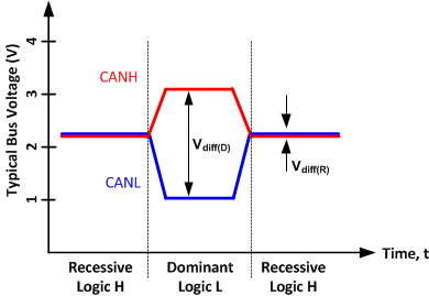 Figure 35. Bus States (Physical Bit Representation)
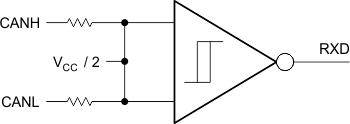 Figure 36. Simplified Recessive Common-Mode Bias and Receiver
These CAN transceivers are typically used in applications with a host microprocessor or FPGA that includes the link layer portion of the CAN protocol. The different nodes on the network are typically connected through the use of a 120-Ω characteristic impedance twisted-pair cable with termination on both ends of the bus.
11.2 Typical Application
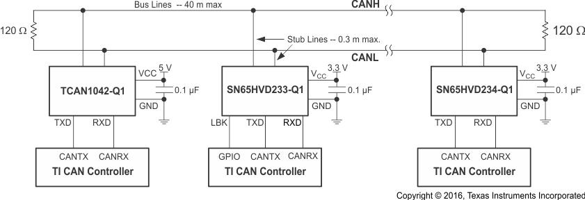 Figure 37. Typical SN65HVD233-Q1 Application
11.2.1 Design Requirements
11.2.1.1 Bus Loading, Length and Number of Nodes
The ISO 11898 standard specifies a data rate of up to 1 Mbps, maximum CAN bus cable length of 40 m, maximum drop line (stub) length of 0.3 m and a maximum of 30 nodes. However, with careful network design, the system may have longer cables, longer stub lengths, and many more nodes to a bus. Many CAN organizations and standards have scaled the use of CAN for applications outside the original ISO 11898 standard. They have made system-level trade-offs for data rate, cable length, and parasitic loading of the bus. Examples of some of these specifications are ARINC825, CANopen, CAN Kingdom, DeviceNet and NMEA200.
A high number of nodes requires a transceiver with high input impedance and wide common-mode range, such as the SN65HVD23x-Q1 CAN family. ISO 11898-2 specifies the driver differential output with a 60-Ω load (two 120-Ω termination resistors in parallel) and the differential output must be greater than 1.5 V. The SN65HVD23x-Q1 devices are specified to meet the 1.5-V requirement with a 60-Ω load, and additionally specified with a differential output voltage minimum of 1.2 V across a common mode range of –2 V to 7 V through a 330-Ω coupling network. This network represents the bus loading of 120 SN65HVD23x-Q1 transceivers based on their minimum differential input resistance of 40 kΩ. Therefore, the SN65HVD23x-Q1 devices support up to 120 transceivers on a single bus segment with margin to the 1.2-V minimum differential input-voltage requirement at each node.
For CAN network design, margin must be given for signal loss across the system and cabling, parasitic loadings, network imbalances, ground offsets and signal integrity. Thus, a practical maximum number of nodes may be lower. Bus length may also be extended beyond the original ISO 11898 standard of 40 m by careful system-design and data-rate tradeoffs. For example, CANopen network design guidelines allow the network to be up to 1 km with changes in the termination resistance, cabling, fewer than 64 nodes, and significantly lowered data rate.
This flexibility in CAN network design is one of the key strengths of the various extensions and additional standards that have been built on the original ISO 11898 CAN standard.
11.2.1.2 CAN Termination
The ISO 11898 standard specifies the interconnect to be a twisted-pair cable (shielded or unshielded) with 120-Ω characteristic impedance (ZO). Resistors equal to the characteristic impedance of the line should be used to terminate both ends of the cable to prevent signal reflections. Unterminated drop lines (stubs) connecting nodes to the bus should be kept as short as possible to minimize signal reflections. The termination may be on the cable or in a node, but if nodes may be removed from the bus the termination must be carefully placed so that it is not removed from the bus.
11.2.2 Detailed Design Procedure
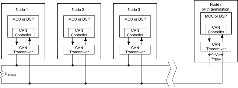 Figure 38. Typical CAN Bus
Termination is typically a 120-Ω resistor at each end of the bus. If filtering and stabilization of the common-mode voltage of the bus is desired, then split termination may be used (see Figure 39). Split termination uses two 60-Ω resistors with a capacitor in the middle of these resistors to ground. Split termination improves the electromagnetic emissions behavior of the network by eliminating fluctuations in the bus common-mode voltages at the start and end of message transmissions.
Care should be taken in the power ratings of the termination resistors used. Typically, the worst-case condition would be if the system power supply is shorted across the termination resistance to ground. In most cases, the current flow through the resistor in this condition would be much higher than the transceiver current limit.
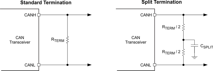 Figure 39. CAN Bus Termination Concepts
11.2.3 Application Curve
Figure 40 shows three typical output waveforms for the SN65HVD233-Q1 device with three different connections made to the RS pin. The top waveform shows the typical differential signal when transitioning from a recessive level to a dominant level on the CAN bus with RS tied to GND through a 0-Ω resistor. The second waveform shows the same signal for the condition with a 10-kΩ resistor tied from RS to ground. The bottom waveform shows the typical differential signal for the case where a 100-kΩ resistor is tied from the RS pin to ground.
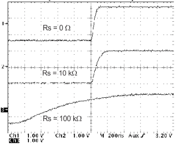 Figure 40. Typical SN65HVD233-Q1 Output Waveforms With Different Slope-Control Resistor Values
11.3 System Example
11.3.1 ISO 11898 Compliance of SN65HVD23x-Q1 Family of 3.3-V CAN Transceivers
11.3.1.1 Introduction
Many users value the low power consumption of operating their CAN transceivers from a 3.3-V supply. However, some are concerned about the interoperability with 5-V-supplied transceivers on the same bus. This report analyzes this situation to address those concerns.
11.3.1.2 Differential Signal
CAN is a differential bus where complementary signals are sent over two wires and the voltage difference between the two wires defines the logical state of the bus. The differential CAN receiver monitors this voltage difference and outputs the bus state with a single-ended logic-level output signal.
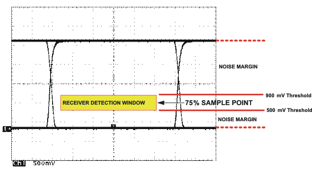 Figure 41. Typical Differential-Output-Voltage Waveform
The CAN driver creates the differential voltage between CANH and CANL in the dominant state. The dominant differential output of the SN65HVD23x-Q1 device is greater than 1.5 V and less than 3 V across a 60-Ω load as defined by the ISO 11898 standard. These are the same limiting values as for 5-V-supplied CAN transceivers. The bus termination resistors, and not the CAN driver, drive the bus to the recessive state.
A CAN receiver is required to output a recessive state when less than 500 mV of differential voltage exists on the bus, and a dominant state when more than 900 mV of differential voltage exists on the bus. The CAN receiver must do this with common-mode input voltages from –2 V to 7 V. The SN65HVD23x-Q1 family of receivers meets these same input specifications as 5-V-supplied receivers do.
11.3.1.3 Common-Mode Signal
The differential receiver rejects the common-mode signal, which is the average of the two CAN signals. The common-mode signal comes from the CAN driver, ground noise, and coupled bus noise. Because the bias voltage of the recessive state of the device is dependent on VCC, any noise present or any variation of VCC has an effect on this bias voltage seen by the bus. The SN65HVD23x-Q1 family has the recessive bias voltage set higher than 0.5 × VCC to comply with the ISO 11898-2 CAN standard. The caveat to this is that the common-mode voltage drops by a approximately 200 millivolts when driving a dominant bit on the bus. This means that there is a common-mode shift between the dominant-bit and recessive-bit states of the device. Although this is not ideal, this small variation in the driver common-mode output is rejected by differential receivers and does not affect data, signal noise margins, or error rates.
11.3.1.4 Interoperability of 3.3-V CAN in 5-V CAN Systems
The 3.3-V-supplied SN65HVD23x-Q1 family of CAN transceivers is fully compatible with 5-V CAN transceivers. The differential output voltage is the same, the recessive common-mode output bias is the same, and the receivers have the same input specifications. The only slight difference is in the dominant common-mode output voltage, which is aapproximately 200 millivolts lower for a 3.3-V CAN transceiver than for a 5-V-supplied transceiver.
To help ensure the widest interoperability possible, the SN65HVD23x-Q1 family has successfully passed the internationally recognized GIFT/ICT conformance and interoperability testing for CAN transceivers. Electrical interoperability does not always assure interchangeability, however. Most implementers of CAN buses recognize that ISO 11898 does not sufficiently specify the electrical layer and that strict standard compliance alone does not ensure full interchangeability. This comes only with thorough equipment testing.