ZHCSEQ7C February 2016 – December 2021 SN65DP141
PRODUCTION DATA
- 1 特性
- 2 应用
- 3 说明
- 4 Revision History
- 5 Pin Configuration and Functions
- 6 Specifications
- 7 Parameter Measurement Information
-
8 Detailed Description
- 8.1 Overview
- 8.2 Functional Block Diagram
- 8.3 Feature Description
- 8.4 Device Functional Modes
- 8.5
Register Maps
- 8.5.1 Register 0x00 (General Device Settings) (offset = 00000000) [reset = 00000000]
- 8.5.2 Register 0x01 (Channel Enable) (offset = 00000000) [reset = 00000000]
- 8.5.3 Register 0x02 (Channel 0 Control Settings) (offset = 00000000) [reset = 00000000]
- 8.5.4 Register 0x03 (Channel 0 Enable Settings) (offset = 00000000) [reset = 00000000]
- 8.5.5 Register 0x05 (Channel 1 Control Settings) (offset = 00000000) [reset = 00000000]
- 8.5.6 Register 0x06 (Channel 1 Enable Settings) (offset = 00000000) [reset = 00000000]
- 8.5.7 Register 0x08 (Channel 2 Control Settings) (offset = 00000000) [reset = 00000000]
- 8.5.8 Register 0x09 (Channel 2 Enable Settings) (offset = 00000000) [reset = 00000000]
- 8.5.9 Register 0x0B (Channel 3 Control Settings) (offset = 00000000) [reset = 00000000]
- 8.5.10 Register 0x0C (Channel 3 Control Settings) (offset = 00000000) [reset = 00000000]
- 9 Application and Implementation
- 10Power Supply Recommendations
- 11Layout
- 12Device and Documentation Support
- 13Mechanical, Packaging, and Orderable Information
9.2.3 Application Curves

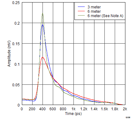
With SN65DP141 -> EQ = 4, VOD = High, ACGain = HiZ, DCGain = Low
Figure 9-3 Cable Mode – Symbol Response
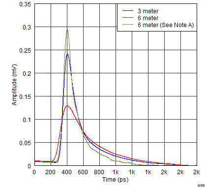
With SN65DP141 -> EQ = 7, VOD = High, ACGain = High, DCGain = Low
Figure 9-5 Trace Mode – Symbol Response
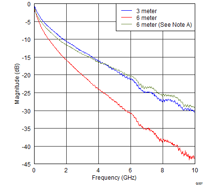
With SN65DP141 -> EQ = 4, VOD = High, ACGain = HiZ, DCGain = Low
Figure 9-4 Cable Mode – Frequency Domain
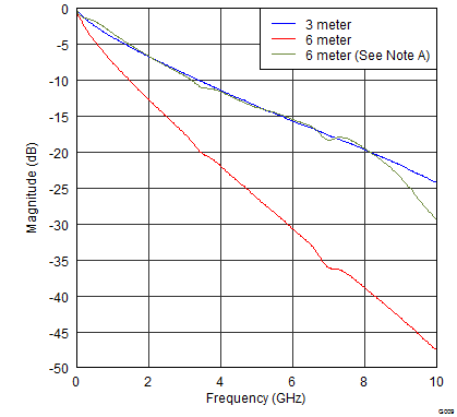
With SN65DP141 -> EQ = 7, VOD = High, ACGain = High, DCGain = Low
Figure 9-6 Trace Mode – Frequency
Domain