ZHCSEQ7C February 2016 – December 2021 SN65DP141
PRODUCTION DATA
- 1 特性
- 2 应用
- 3 说明
- 4 Revision History
- 5 Pin Configuration and Functions
- 6 Specifications
- 7 Parameter Measurement Information
-
8 Detailed Description
- 8.1 Overview
- 8.2 Functional Block Diagram
- 8.3 Feature Description
- 8.4 Device Functional Modes
- 8.5
Register Maps
- 8.5.1 Register 0x00 (General Device Settings) (offset = 00000000) [reset = 00000000]
- 8.5.2 Register 0x01 (Channel Enable) (offset = 00000000) [reset = 00000000]
- 8.5.3 Register 0x02 (Channel 0 Control Settings) (offset = 00000000) [reset = 00000000]
- 8.5.4 Register 0x03 (Channel 0 Enable Settings) (offset = 00000000) [reset = 00000000]
- 8.5.5 Register 0x05 (Channel 1 Control Settings) (offset = 00000000) [reset = 00000000]
- 8.5.6 Register 0x06 (Channel 1 Enable Settings) (offset = 00000000) [reset = 00000000]
- 8.5.7 Register 0x08 (Channel 2 Control Settings) (offset = 00000000) [reset = 00000000]
- 8.5.8 Register 0x09 (Channel 2 Enable Settings) (offset = 00000000) [reset = 00000000]
- 8.5.9 Register 0x0B (Channel 3 Control Settings) (offset = 00000000) [reset = 00000000]
- 8.5.10 Register 0x0C (Channel 3 Control Settings) (offset = 00000000) [reset = 00000000]
- 9 Application and Implementation
- 10Power Supply Recommendations
- 11Layout
- 12Device and Documentation Support
- 13Mechanical, Packaging, and Orderable Information
6.6 Switching Characteristics
over operating free-air temperature range (unless otherwise noted)
| PARAMETER | TEST CONDITIONS | MIN | TYP | MAX | UNIT | |
|---|---|---|---|---|---|---|
| CML OUTPUTS (OUT[3:0]_P, OUT[3:0]_N) | ||||||
| tR | Rise time (1) | Input signal with 30 ps rise time, 20% to 80%, See Figure 7-3 | 31 | ps | ||
| tF | Fall time (1) | Input signal with 30 ps fall time, 20% to 80%, See Figure 7-3 | 32 | ps | ||
| SDD22 | Differential output return loss | 6 GHz (12 Gbps) | -14 | dB | ||
| 4.05 GHz (HBR3, 8.1 Gbps) | –9.33 | dB | ||||
| 4.05 GHz (HBR3, 8.1 Gbps) | –6.35 | dB | ||||
| 1.35 GHz (HBR, 2.7Gbps) | –3.5 | dB | ||||
| tPLH | Low-to-high propagation delay | See Figure 7-2 | 65 | ps | ||
| tPHL | High-to-low propagation delay | 65 | ps | |||
| tSK(O) | Inter-Pair (lane to lane) output skew (2) | All outputs terminated with 100 Ω, See Figure 7-4 | 8 | ps | ||
| tSK(PP) | Part-to-part skew (3) | All outputs terminated with 100 Ω | 50 | ps | ||
| rOT | Single ended output resistance | Single ended on-chip termination to VCC, Outputs are AC coupled | 50 | Ω | ||
| rOM | Output termination mismatch at 1 MHz | 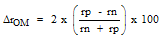 | 5% | |||
| Channel-to-channel isolation | Frequency at 6 GHz | 35 | 45 | dB | ||
| Output referred noise(4) | 10 MHz to 6 GHz, No other noise source present, VOD = LOW | 400 | µVRMS | |||
| 10 MHz to 6 GHz, No other noise source present, VOD = HIGH | 500 | µVRMS | ||||
| EQUALIZATION | ||||||
| G | At 6 GHz input signal | Equalization Gain, EQ = MAX | 15 | dB | ||
| V(pre) | Output pre-cursor pre-emphasis | Input signal with 3.75 pre-cursor and measure it on the output signal, See Figure 7-5 | 3.75 | dB | ||
| V(pst) | Output post-cursor pre-emphasis | Input signal with 12 dB post-cursor and measure it on the output signal, See Figure 7-5 | 12 | dB | ||
(1) Rise and Fall measurements include board and channel effects of the test environment, refer to Figure 7-1 and Figure 7-3.
(2) tSK(O) is the magnitude of the time difference between the channels.
(3) tSK(PP) is the magnitude of the difference in propagation delay times between any specified terminals of two devices when both devices operate with the same
(4) All noise sources added.