ZHCSEQ7C February 2016 – December 2021 SN65DP141
PRODUCTION DATA
- 1 特性
- 2 应用
- 3 说明
- 4 Revision History
- 5 Pin Configuration and Functions
- 6 Specifications
- 7 Parameter Measurement Information
-
8 Detailed Description
- 8.1 Overview
- 8.2 Functional Block Diagram
- 8.3 Feature Description
- 8.4 Device Functional Modes
- 8.5
Register Maps
- 8.5.1 Register 0x00 (General Device Settings) (offset = 00000000) [reset = 00000000]
- 8.5.2 Register 0x01 (Channel Enable) (offset = 00000000) [reset = 00000000]
- 8.5.3 Register 0x02 (Channel 0 Control Settings) (offset = 00000000) [reset = 00000000]
- 8.5.4 Register 0x03 (Channel 0 Enable Settings) (offset = 00000000) [reset = 00000000]
- 8.5.5 Register 0x05 (Channel 1 Control Settings) (offset = 00000000) [reset = 00000000]
- 8.5.6 Register 0x06 (Channel 1 Enable Settings) (offset = 00000000) [reset = 00000000]
- 8.5.7 Register 0x08 (Channel 2 Control Settings) (offset = 00000000) [reset = 00000000]
- 8.5.8 Register 0x09 (Channel 2 Enable Settings) (offset = 00000000) [reset = 00000000]
- 8.5.9 Register 0x0B (Channel 3 Control Settings) (offset = 00000000) [reset = 00000000]
- 8.5.10 Register 0x0C (Channel 3 Control Settings) (offset = 00000000) [reset = 00000000]
- 9 Application and Implementation
- 10Power Supply Recommendations
- 11Layout
- 12Device and Documentation Support
- 13Mechanical, Packaging, and Orderable Information
11.1 Layout Guidelines
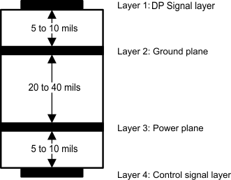
- Placing a solid ground plane next to the high-speed signal layer establishes controlled impedance for transmission line interconnects and provides an excellent low-inductance path for the return current flow.
- Placing the power plane next to the ground plane creates additional high-frequency bypass capacitance.
- Routing the slower speed control signals on the bottom layer allows for greater flexibility as these signal links usually have margin to tolerate discontinuities such as vias.
- If an additional supply voltage plane or signal layer is needed, add a second power/ground plane system to the stack to keep it symmetrical. This makes the stack mechanically stable and prevents it from warping. Also the power and ground plane of each power system can be placed closer together, thus increasing the high frequency bypass capacitance significantly.
- The control pin pull-up and pull-down resistors are shown in application section for reference. If a high level is needed then only uses the pull up. If a low level is needed only use the pull down.
- Place passive components within the signal path, such as source-matching resistors or ac-coupling capacitors, next to each other. Routing as in case a) creates wider trace spacing than in b); the resulting discontinuity, however, is limited to a far narrower area.
- When routing traces next to a via or between an array of vias, make sure that the via clearance section does not interrupt the path of the return current on the ground plane below.
- Avoid metal layers and traces underneath or between the pads off the DisplayPort connectors for better impedance matching. Otherwise they will cause the differential impedance to drop below 75 Ω and fail the board during TDR testing.
- Use solid power and ground planes for 100 Ω impedance control and minimum power noise.
- For a multi-layer PCB, it is recommended to keep one common GND layer underneath the device and connect all ground terminals directly to this plane. For 100 Ω differential impedance, use the smallest trace spacing possible, which is usually specified by the PCB vendor.
- Keep the trace length as short as possible to minimize attenuation.
- Place bulk capacitors (that is, 10 μF) close to power sources, such as voltage regulators or where the power is supplied to the PCB.
 Figure 11-1 PCB Stack