SNVS857 February 2014 LP8555
PRODUCTION DATA.
- 1 Features
- 2 Applications
- 3 Description
- 4 Simplified Schematic
- 5 Revision History
- 6 Terminal Configuration and Functions
- 7 Specifications
-
8 Detailed Description
- 8.1 Overview
- 8.2 Functional Block Diagram
- 8.3
Features Description
- 8.3.1 Boost Converter Overview
- 8.3.2 Brightness Control
- 8.3.3 LED Brightness Slopes, Normal and Advanced
- 8.3.4
Start-up and Shutdown Sequences
- 8.3.4.1 Start-up With PWM Input Brightness Control Mode (BRTMODE = 00b)
- 8.3.4.2 Shutdown With PWM Input Brightness Control Mode (BRTMODE = 00b)
- 8.3.4.3 Start-up With I2C Brightness Control Mode (BRTMODE = 01b)
- 8.3.4.4 Shutdown With I2C Brightness Control Mode (BRTMODE = 01b)
- 8.3.4.5 Start-up with I2C + PWM Input Brightness Control Mode (BRTMODE = 10 or 11b)
- 8.3.4.6 Shutdown with I2C + PWM Input Brightness Control Mode (BRTMODE = 10 or 11b)
- 8.3.5 LED String Count Auto Detection
- 8.3.6 Fault Detection
- 8.3.7 I2C-Compatible Serial Bus Interface
- 8.4 Device Functional Modes
- 8.5
Register Maps
- 8.5.1 COMMAND
- 8.5.2 STATUS/MASK
- 8.5.3 BRTLO
- 8.5.4 BTHI
- 8.5.5 CONFIG
- 8.5.6 CURRENT
- 8.5.7 PGEN
- 8.5.8 BOOST
- 8.5.9 LEDEN
- 8.5.10 STEP
- 8.5.11 Brightness Transitions, Typical Times
- 8.5.12 VOLTAGE_0
- 8.5.13 LEDEN1
- 8.5.14 VOLTAGE1
- 8.5.15 OPTION
- 8.5.16 EXTRA
- 8.5.17 ID
- 8.5.18 REVISION
- 8.5.19 CONF0
- 8.5.20 CONF1
- 8.5.21 VHR0
- 8.5.22 VHR1
- 8.5.23 JUMP
-
9 Application and Implementation
- 9.1 Application Information
- 9.2 Typical Applications
- 10Power Supply Recommendations
- 11Layout
- 12 Device and Documentation Support
- 13Mechanical, Packaging, and Orderable Information
6 Terminal Configuration and Functions
YFQ (DSBGA)
36 Bumps
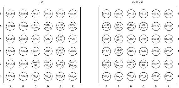
Terminal Functions
| TERMINAL | TYPE | DESCRIPTION | |
|---|---|---|---|
| NUMBER | NAME | ||
| A1, A2, A3, B1, B2, B3, | LEDAx | A | LED Bank A Current Sink Terminal. If unused, this terminal may be left floating. |
| A4, A5, A6, B4, B5, B6 | LEDBx | A | LED Bank A Current Sink Terminal. If unused, this terminal may be left floating. |
| C1 | FB_A | A | Feedback terminal for the Bank A Boost Converter. |
| C2 | PWM/INT | I | Dual function terminal. When BRTMODE = 00, 10, or 11, this is a PWM input terminal. When BRTMODE = 01, this terminal is a programmable interrupt terminal. In this mode, this is an open drain output that pulls low when a fault condition occurs. |
| C3, C4, D3, D4 | GND | G | Ground for analog and digital blocks. These terminals should be connected to a noise-free GND plane if possible (separate plane than GND_SW_x terminals). |
| C5 | EN/VDDIO | I | Backlight Enable terminal and VDDIO power terminal + reference terminal for I2C communication. This terminal should be connected to IO voltage with low impedance route to avoid voltage ripple on this terminal. |
| C6 | FB_B | A | Feedback terminal for the Bank B Boost Converter. |
| D1, E1, F1 | SW_A | A | Bank A Boost Converter Switch |
| D2, E2, F2 | GND_SW_A | G | Bank A Boost Converter Switch Ground. These terminals can be connected to noisy GND due to high current spikes. |
| D5, E5, F5 | GND_SW_B | G | Bank B Boost Converter Switch Ground. These terminals can be connected to noisy GND due to high current spikes. |
| D6, E6, F6 | SW_B | A | Bank B Boost Converter Switch |
| E3 | FSET/SDA | I/O/A | Dual Function terminal. When I2C is not used (for example, BRTMODE = 00), this terminal can be used to set the boost switching frequency and/or LED PWM frequency by connecting a resistor between the terminal and a ground reference. When I2C is used (for example, BRTMODE = 01, 10, or 11), this terminal is connected to a SDA line of an I2C bus. |
| E4 | ISET/SCL | I/A | Dual Function terminal. When I2C is not used (for example, if BRTMODE=00), this terminal can be used to set the full-scale LED current by connecting a resistor between the terminal and a ground reference. When I2C is used (for example, BRTMODE = 01, 10, or 11), this terminal is connected to a SCL line of an I2C bus. |
| F3 | VLDO | P | Internal LDO Output terminal. CVLDO bypass capacitor must be connected between this terminal and ground. |
| F4 | VDD | P | Device power supply terminal. Provide 2.7-V to 20-V supply to this terminal. This terminal is an input of the internal LDO regulator. The output of the internal LDO powers the device blocks. |
| A: Analog, G: Ground Terminal, P: Power Terminal, I: Input Terminal, O: Output Terminal | |||