SNVS857 February 2014 LP8555
PRODUCTION DATA.
- 1 Features
- 2 Applications
- 3 Description
- 4 Simplified Schematic
- 5 Revision History
- 6 Terminal Configuration and Functions
- 7 Specifications
-
8 Detailed Description
- 8.1 Overview
- 8.2 Functional Block Diagram
- 8.3
Features Description
- 8.3.1 Boost Converter Overview
- 8.3.2 Brightness Control
- 8.3.3 LED Brightness Slopes, Normal and Advanced
- 8.3.4
Start-up and Shutdown Sequences
- 8.3.4.1 Start-up With PWM Input Brightness Control Mode (BRTMODE = 00b)
- 8.3.4.2 Shutdown With PWM Input Brightness Control Mode (BRTMODE = 00b)
- 8.3.4.3 Start-up With I2C Brightness Control Mode (BRTMODE = 01b)
- 8.3.4.4 Shutdown With I2C Brightness Control Mode (BRTMODE = 01b)
- 8.3.4.5 Start-up with I2C + PWM Input Brightness Control Mode (BRTMODE = 10 or 11b)
- 8.3.4.6 Shutdown with I2C + PWM Input Brightness Control Mode (BRTMODE = 10 or 11b)
- 8.3.5 LED String Count Auto Detection
- 8.3.6 Fault Detection
- 8.3.7 I2C-Compatible Serial Bus Interface
- 8.4 Device Functional Modes
- 8.5
Register Maps
- 8.5.1 COMMAND
- 8.5.2 STATUS/MASK
- 8.5.3 BRTLO
- 8.5.4 BTHI
- 8.5.5 CONFIG
- 8.5.6 CURRENT
- 8.5.7 PGEN
- 8.5.8 BOOST
- 8.5.9 LEDEN
- 8.5.10 STEP
- 8.5.11 Brightness Transitions, Typical Times
- 8.5.12 VOLTAGE_0
- 8.5.13 LEDEN1
- 8.5.14 VOLTAGE1
- 8.5.15 OPTION
- 8.5.16 EXTRA
- 8.5.17 ID
- 8.5.18 REVISION
- 8.5.19 CONF0
- 8.5.20 CONF1
- 8.5.21 VHR0
- 8.5.22 VHR1
- 8.5.23 JUMP
-
9 Application and Implementation
- 9.1 Application Information
- 9.2 Typical Applications
- 10Power Supply Recommendations
- 11Layout
- 12 Device and Documentation Support
- 13Mechanical, Packaging, and Orderable Information
9 Application and Implementation
9.1 Application Information
The LP8555 designed for LCD backlighting, especially for high-resolution tablet panels where more backlight power is needed due to smaller aperture ratio of the LCD. With single-boost configuration the inductor selection is difficult for height restricted applications; to overcome this LP8555 uses dual-boost configuration. This shares the total load to two boost inductors and allows using two smaller inductors instead of one large inductor while maintaining good efficiency. 12 LED current sinks allow driving up to 96 LEDs with high efficiency. Better efficiency is achieved with using lower conversion ratio for boost and driving more LEDs in parallel, compared to using fewer LED strings and higher boost conversion ratio. Main limiting factor for output power is inductor current limit, which is calculated in the Detailed Design Procedure. PCB thermal performance must be considered in high power applications where thermal dissipation of LP8555 can become limiting factor.
Due to a flexible input voltage configuration, the LP8555 can be used also in various other applications, such as laptop backlighting, as well as other LED lighting where high number of LEDs are needed and must be driven with highest possible efficiency. The following design procedure can be used to select component values for the LP8555. An example for default EPROM configuration is given with corresponding design parameters. LP8555EVM User Guide has reference bill of materials and example layout pictures.
9.2 Typical Applications
9.2.1 Application for Default LP8555YFQR EPROM Configuration
With the default EPROM configuration PWM input is used for brightness control. The backlight is enabled/disabled and also configuration can be changed before backlight turning on with I2C writes. Up to 12 LED strings can be used with max 28-V boost output voltage. LED current is set to 25 mA by default. See detailed EPROM setup in LP8555YFQR EPROM Configuration.
9.2.1.1 Schematic
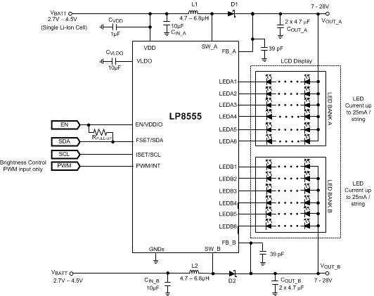 Figure 43. Application Diagram for Default EPROM Setup
9.2.1.2 LP8555YFQR EPROM Configuration
| ADDRESS (HEX) | BIT | BIT NAME | BIT DESCRIPTION | VALUE | MEANING | REG VALUE (HEX) |
|---|---|---|---|---|---|---|
| 00 | 2 | SREN | Boost slew rate limit enable | 0b | 0 = Boost slew rate not limited | 00 |
| 1 | SSEN | Spread spectrum enable | 0b | 0 = Spread spectrum disabled | ||
| 0 | ON | Backlight enable | 0b | 0 = Backlight enabled only by writing this bit to 1 | ||
| 10 | 7 | PWMSB | Enable automatic PWM input shutdown | 0b | 0 = Shutdown function disabled | 64 |
| 6 | PWMFILT | Enable PWM input filtering | 1b | 1 = PWM input analog 50 ns filter enabled | ||
| 5 | EN_BPHASE180 | Enable boost 180° phase difference | 1b | 1 = Boosts clocks are 180° shifted | ||
| 4 | - | 0b | ||||
| 3 | RELOAD | Enable EPROM read at every BL enable sequence | 0b | 0 = EPROM is read only at first start-up | ||
| 2 | AUTO | Enable auto detect for number of LEDs during start-up | 1b | 1 = LED string auto detection enabled | ||
| 1:0 | BRTMODE | Brightness control mode | 00b | 00 = PWM input duty control only | ||
| 11 | 7 | ISET | Enable external resistor setting of LED string current | 0b | 0 = LED current set with registers | 05 |
| 6:3 | - | 0000b | ||||
| 2:0 | MAXCURR | Set maximum DC current per string | 101b | 101 = 25 mA | ||
| 12 | 7 | PFSET | Enable external resistor PWM frequency setting | 0b | 0 = PWM frequency selected with registers | 2B |
| 6 | - | 0b | ||||
| 5:3 | THRESHOLD | Hybrid PMW and Current Control switch point control | 101b | 101 = 25% switch point | ||
| 2:0 | PFSET | PWM frequency selection | 011b | 011 = 19.5 kHz | ||
| 13 | 7 | - | 0b | 01 | ||
| 6 | - | 0b | ||||
| 5:2 | - | 0000b | ||||
| 1 | BIND | Boost inductor selection | 0b | 0 = 4.7 µH ... 6.8 µH inductor | ||
| 0 | BFREQ | Boost SW frequency | 1b | 1 = 1 MHz | ||
| 14 | 7:6 | OV | Set LED high comparator detection level | 10b | 10 = 3 V | BF |
| 5:0 | ENABLE_0 | LED bank A string enable | 111111b | 1 = Enabled (all six strings) | ||
| 15 | 7:6 | SMOOTH | Advanced Sloping smoothing factor | 00b | 00 = No smoothing | 20 |
| 5:3 | PWM_IN_HYST | PWM input hysteresis | 100b | 100 = >8 LSB steps | ||
| 2:0 | STEP | Linear Slope time | 000b | 000 = 0ms | ||
| 16 | 7:6 | VMAX_0 | Bank A boost maximum voltage | 11b | 11 = 28 V | F8 |
| 5 | ADAPT_0 | Enable boost adaptive control for bank A | 1b | 1 = Adaptive headroom enabled | ||
| 4:0 | VINIT_0 | Initial voltage for bank A boost | 11000b | 11000 = 23.26 V | ||
| 19 | 5:0 | ENABLE_1 | LED bank B string enable | 111111b | 1 = Enabled (all six strings) | 3F |
| 1A | 7 | VMAX_1 | Bank B boost maximum voltage | 11b | 11 = 28 V | F8 |
| 6 | ADAPT_1 | Enable boost adaptive control for bank B | 1b | 1 = Adaptive headroom enabled | ||
| 5 | VINIT_1 | Initial voltage for bank B boost | 11000b | 11000 = 23.26 V | ||
| 1E | 7:4 | ID_CUST | ID register, Customer ID | 0000b | 0000 | 00 |
| 3:0 | ID_CFG | ID register, EPROM config | 0000b | 0000 | ||
| 76 | 7 | BOOST_IS_DIV2 | Option divide Imax peak current by 2 | 0b | 0 = Normal current limit | 0B |
| 6:5 | - | 00b | ||||
| 4 | ALTID | I2C slave ID selector | 0b | 0 = 2Ch (7-bit) | ||
| 3:2 | SRON | Slowed boost slew rate | 10b | When COMMAND.SREN is set to 1 this value is used. 10 = Second slowest |
||
| 1:0 | CURR_LIMIT | Inductor peak current limit | 11b | 11 = 3.1 A | ||
| 77 | 7:6 | FMOD_DIV | Spread spectrum modulation frequency divisor | 00b | When COMMAND.SSEN is set to 1 this value is used. 00 = 0.42% |
17 |
| 5:0 | - | 010111b | ||||
| 78 | 6:4 | VHR_SLOPE | LED driver maximum headroom voltage at maximum current (50mA) | 110b | 110 = 285 mV | 60 |
| 3 | - | 0b | ||||
| 2:0 | VHR_VERT | LED driver maximum headroom voltage at minimum current | 000b | 000 = 50 mV | ||
| 79 | 5:4 | VHR_HYST | LED driver hysteresis for mid comparator level | 01b | 01 = 233 mV | 11 |
| 3:2 | - | 00b | ||||
| 1:0 | VHR_HORZ | LED driver headroom control knee percentage of full LED current | 01b | 01 = 25% | ||
| 7A | 7 | JEN | Enable boost voltage jumping on brightness change | 1b | 1 = Jump enabled | 88 |
| 6:4 | - | 000b | ||||
| 3:2 | JTHR | Jump brightness threshold | 10b | 10 = 25% | ||
| 1:0 | JVOLT | Jump voltage | 00b | 00 = 2 V |
9.2.1.3 Design Requirements
Example requirements based on default EPROM setup.
| DESIGN PARAMETER | EXAMPLE VALUE |
|---|---|
| Input voltage range | 2.7 V to 4.5 V (Single Li-Ion cell battery) |
| Brightness Control | PWM input duty cycle |
| Backlight enabled | Writing ON bit 1 with I2C |
| PWM output frequency | 19.2 kHz with PSPWM enabled |
| LED Current | 25 mA / channel |
| Number of Channels | Up to 12 with string auto detection enabled |
| Brightness slopes | Disabled |
| External set resistors | Disabled |
| Inductor | 4.7 µH to 6.8 µH, at least 3.1-A saturation current |
| Boost SW frequency | 1 MHz |
| Maximum output voltage | 28 V |
| SW current limit | 3.1 A |
| CABC | Jump enabled for >25% brightness changes |
9.2.1.4 Detailed Design Procedure
9.2.1.4.1 Inductor
There are two main considerations when choosing an inductor; the inductor should not saturate, and the inductor current ripple should be small enough to achieve the desired output voltage ripple. Different saturation current rating specifications are followed by different manufacturers so attention must be given to details. Saturation current ratings are typically specified at 25°C. However, ratings at the maximum ambient temperature of application should be requested from the manufacturer. Shielded inductors radiate less noise and should be preferred.
The saturation current should be greater than the sum of the maximum load current and the worst case average to peak inductor current.
Figure 44 shows the worst case conditions.
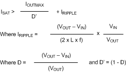 Figure 44. Calculating Inductor Maximum Current
- IRIPPLE: peak inductor current
- IOUTMAX: maximum load current
- VIN: minimum input voltage in application
- L : min inductor value including worst case tolerances
- f : minimum switching frequency
- VOUT: output voltage
- D: Duty Cycle for CCM Operation
- VOUT : Output Voltage
As a result the inductor should be selected according to the ISAT. A more conservative and recommended approach is to choose an inductor that has a saturation current rating greater than the maximum current limit of 3.1 A. A 4.7-µH to 6.8-µH inductor with a saturation current rating of at least 3.1 A is recommended for most applications. The inductor’s resistance should be less than 300 mΩ for good efficiency.
9.2.1.4.2 Output Capacitor
A ceramic capacitor with 50-V voltage rating is recommended for the output capacitor. The DC-bias effect can reduce the effective capacitance by up to 80% especially with small package size capacitors, which needs to be considered in capacitance value and package selection. Typically one 10-µF or two 4.7-µF capacitors is sufficient. Effectively the capacitance should be at least 2 µF at boost maximum output voltage.
9.2.1.4.3 LDO Capacitor
A ceramic capacitor with at least 10 V voltage rating is recommended for the output capacitor of the LDO. The DC-bias effect can reduce the effective capacitance by up to 80%, which needs to be considered in capacitance value selection. Typically 10 µF capacitor is sufficient.
9.2.1.4.4 VDD Capacitor
A ceramic capacitor with at least 10-V voltage rating is recommended for the VDD input capacitor. If input voltage is higher, then the rating should be selected accordingly. The DC-bias effect can reduce the effective capacitance by up to 80%, which needs to be considered in capacitance value selection. Typically, a 1-μF capacitor is sufficient. X5R/X7R are recommended types.
9.2.1.4.5 Boost Input Capacitor
A ceramic capacitor with at least 10-V voltage rating is recommended for the boost input capacitor. If input voltage is higher, then the rating should be selected accordingly. The DC-bias effect can reduce the effective capacitance by up to 80%, which needs to be considered in capacitance value selection. Typically, a 10-μF capacitor per boost is sufficient. X5R/X7R are recommended types.
9.2.1.4.6 Diode
A Schottky diode should be used for the output diode. Peak repetitive current should be greater than inductor peak current (3.1 A) to ensure reliable operation. Average current rating should be greater than the maximum output current. Schottky diodes with a low forward drop and fast switching speeds are ideal for increasing efficiency in portable applications. Choose a reverse breakdown voltage of the Schottky diode significantly larger (~40 V) than the output voltage. Do not use ordinary rectifier diodes, since slow switching speeds and long recovery times cause the efficiency and the load regulation to suffer.
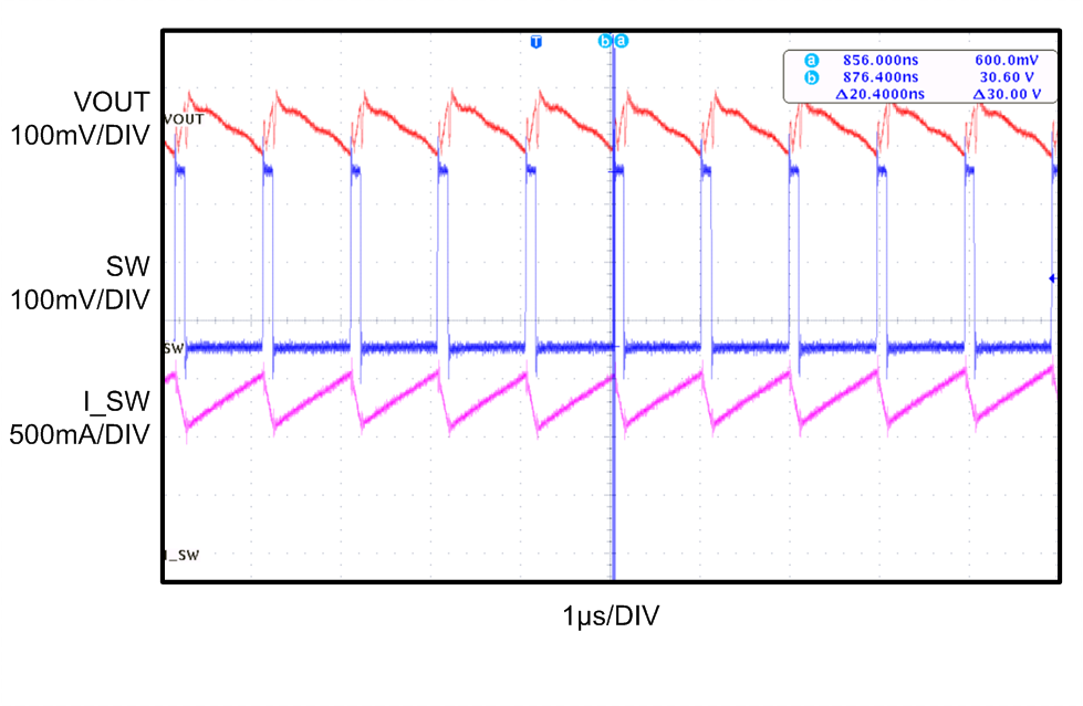
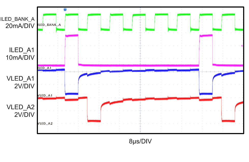
9.2.1.5 Application Performance Plots
Typical performance plots with default EPROM configuration. The LP8555EVM was used for taking the oscilloscope plots.
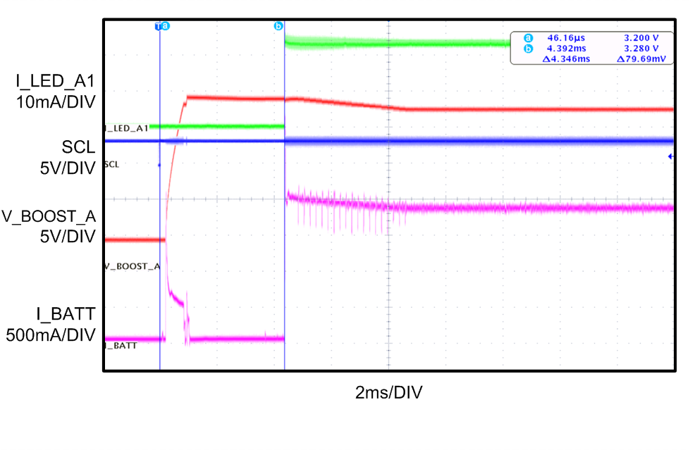
| VDD = 3.7V | ILED = 25 mA | 12 x 7 LEDs |
Full Brightness Slope Function Disabled.
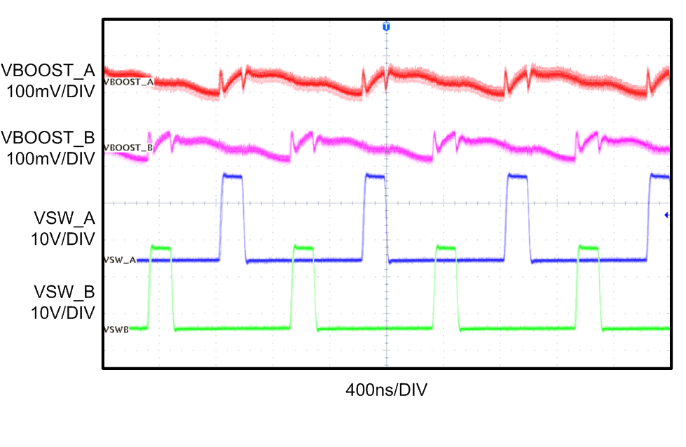
| VDD = 3.7V | fSW = 1 MHz |
| VDD = 3.7V | VBOOST = 28V | Load = 150 mA |
| ƒPWM = 19.5 kHz | 6 Strings |
9.2.2 Application Example With Different LED Configuration for Each Bank
In the following example schematic it is shown how the LED banks can have different LED configuration. Bank A has 4 active LED outputs and Bank B has 5 active LED outputs. LP8555 will automatically detect open outputs and adjust phase shifting for both banks optimally. Control in this example is from I2C bus and PWM/INT terminal is used for interrupt signal, notifying processor on possible fault conditions. Component selection and performance plots follow the examples shown in first application example with default EPROM configuration, but the PSPWM is adjusted based on the number of connected strings. Details on I2C registers and EPROM settings are seen in the Register Map section. If custom EPROM is required, please contact TI Sales representative for availability.
9.2.2.1 Schematic
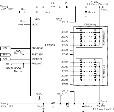 Figure 49. Application Example With Different LED Configurations on Each Bank
9.2.3 Application Example With 12 LED Strings and PWM Input Brightness Control
In the following example schematic it is shown how the LP8555 can be configured for operating without I2C control. Only controls needed are PWM input for brightness control and EN for enabling and disabling device. PWM frequency is set with RFSET resistor and LED current is set with ISET resistor. Full 12 channels are used in this example, but other configurations can be used as well. Component selection and performance plots follow the examples shown in first application example with default EPROM configuration. Details on I2C registers and EPROM settings are seen in the Register Map section. If custom EPROM is required, please contact TI Sales representative for availability. Since this configuration relies on pre-programmed EPROM for basic setup (although LED current and PWM frequency are set with resistors), special EPROM configuration is needed for this application.
9.2.3.1 Schematic
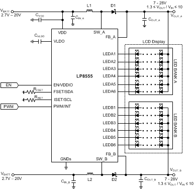 Figure 50. Application Example with 12 LED Strings and PWM Input Brightness Control
9.2.4 Application With 12 LED Strings, I2C Brightness Control
In the following example full 12 channels are used with I2C brightness control. PWM/INT terminal is used for interrupt signal, notifying processor on possible fault conditions. LED current and PWM frequency are set with I2C writes, or default EPROM values can be used as well. Component selection and performance plots follow the examples shown in first application example with default EPROM configuration. Configuration registers can be set before backlight is enabled, so special pre-set EPROM is not necessarily needed. Details on I2C registers and EPROM settings are seen in the Register Map section. If custom EPROM is required, please contact TI Sales representative for availability.
9.2.4.1 Schematic
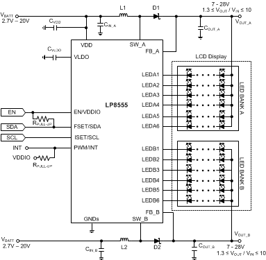 Figure 51. Application Example With 12 LED Strings, I2C Brightness Control