SNVS857 February 2014 LP8555
PRODUCTION DATA.
- 1 Features
- 2 Applications
- 3 Description
- 4 Simplified Schematic
- 5 Revision History
- 6 Terminal Configuration and Functions
- 7 Specifications
-
8 Detailed Description
- 8.1 Overview
- 8.2 Functional Block Diagram
- 8.3
Features Description
- 8.3.1 Boost Converter Overview
- 8.3.2 Brightness Control
- 8.3.3 LED Brightness Slopes, Normal and Advanced
- 8.3.4
Start-up and Shutdown Sequences
- 8.3.4.1 Start-up With PWM Input Brightness Control Mode (BRTMODE = 00b)
- 8.3.4.2 Shutdown With PWM Input Brightness Control Mode (BRTMODE = 00b)
- 8.3.4.3 Start-up With I2C Brightness Control Mode (BRTMODE = 01b)
- 8.3.4.4 Shutdown With I2C Brightness Control Mode (BRTMODE = 01b)
- 8.3.4.5 Start-up with I2C + PWM Input Brightness Control Mode (BRTMODE = 10 or 11b)
- 8.3.4.6 Shutdown with I2C + PWM Input Brightness Control Mode (BRTMODE = 10 or 11b)
- 8.3.5 LED String Count Auto Detection
- 8.3.6 Fault Detection
- 8.3.7 I2C-Compatible Serial Bus Interface
- 8.4 Device Functional Modes
- 8.5
Register Maps
- 8.5.1 COMMAND
- 8.5.2 STATUS/MASK
- 8.5.3 BRTLO
- 8.5.4 BTHI
- 8.5.5 CONFIG
- 8.5.6 CURRENT
- 8.5.7 PGEN
- 8.5.8 BOOST
- 8.5.9 LEDEN
- 8.5.10 STEP
- 8.5.11 Brightness Transitions, Typical Times
- 8.5.12 VOLTAGE_0
- 8.5.13 LEDEN1
- 8.5.14 VOLTAGE1
- 8.5.15 OPTION
- 8.5.16 EXTRA
- 8.5.17 ID
- 8.5.18 REVISION
- 8.5.19 CONF0
- 8.5.20 CONF1
- 8.5.21 VHR0
- 8.5.22 VHR1
- 8.5.23 JUMP
-
9 Application and Implementation
- 9.1 Application Information
- 9.2 Typical Applications
- 10Power Supply Recommendations
- 11Layout
- 12 Device and Documentation Support
- 13Mechanical, Packaging, and Orderable Information
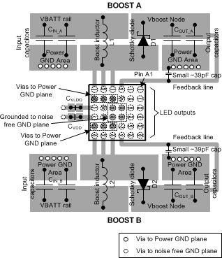
11 Layout
11.1 Layout Guidelines
In Layout Example is a layout recommendation for LP8555. The figure is used for demonstrating the principle of good layout. This layout can be adapted to the actual application layout if/where possible.
It is important that all boost components are close to the chip and the high current traces should be wide enough. By placing one boost component on one side of the chip it is easy to keep the ground plane intact below the high current paths. This way other chip terminals can be routed more easily without splitting the ground plane. VDD and VLDO need to be as noise-free as possible. Place the bypass capacitors near the corresponding terminals and ground them to as noise-free ground as possible.
Here are some main points to help the PCB layout work:
- Current loops need to be minimized:
- For low frequency the minimal current loop can be achieved by placing the boost components as close to the SW and SW_GND terminals as possible. Input and output capacitor grounds need to be close to each other to minimize current loop size.
- Minimal current loops for high frequencies can be achieved by making sure that the ground plane is intact under the current traces. High frequency return currents try to find route with minimum impedance, which is the route with minimum loop area, not necessarily the shortest path. Minimum loop area is formed when return current flows just under the “positive” current route in the ground plane, if the ground plane is intact under the route. Traces from inner pads of the LP8555 need to be routed from below the part in the inner layer so that traces do not split the ground plane under the boost traces or components.
- GND plane needs to be intact under the high current boost traces to provide shortest possible return path and smallest possible current loops for high frequencies.
- Current loops when the boost switch is conducting and not conducting needs to be on the same direction in optimal case.
- Inductor placement should be so that the current flows in the same direction as in the current loops. Rotating inductor 180° changes current direction.
- Use separate power and noise free grounds. Power ground is used for boost converter return current and noise free ground for more sensitive signals, like VDD and VLDO bypass capacitor grounding as well as grounding the GND terminals of LP8555 itself.
- Boost output feedback voltage to LEDs need to be taken out “after” the output capacitors, not straight from the diode cathode.
- A small (for example, 39 pF) bypass capacitor should be placed close to the FB terminal(s) to suppress high frequency noise
- VDD line should be separated from the high current supply path to the boost converter(s) to prevent high frequency ripple affecting the chip behavior. A separate 1-µF bypass capacitor is used for the VDD terminal, and it is grounded to noise-free ground.
- Input and output capacitors need strong grounding (wide traces, many vias to GND plane)
- If two output capacitors are used they need symmetrical layout to get both capacitors working ideally
- Output capacitors DC-bias effect. If the output capacitance is too low, it can cause boost to become instable on some loads and this increases EMI. DC bias characteristics need to be obtained from the component manufacturer; it is not taken into account on component tolerance. X5R/X7R capacitors are recommended.
11.2 Layout Example