ZHCSDN1E August   2012  – September 2021 LMZ20501

PRODUCTION DATA  

  1. 特性
  2. 应用
  3. 说明
  4. Revision History
  5. Pin Configuration and Functions
  6. Specifications
    1. 6.1 Absolute Maximum Ratings
    2. 6.2 ESD Ratings
    3. 6.3 Recommended Operating Conditions
    4. 6.4 Thermal Information
    5. 6.5 Electrical Characteristics
    6. 6.6 System Characteristics
    7. 6.7 Typical Characteristics
  7. Detailed Description
    1. 7.1 Overview
    2. 7.2 Functional Block Diagram
    3. 7.3 Feature Description
      1. 7.3.1 Nano Scale Package
      2. 7.3.2 Internal Synchronous Rectifier
      3. 7.3.3 Current Limit Protection
      4. 7.3.4 Start-Up
      5. 7.3.5 Dropout Behavior
      6. 7.3.6 Power Good Flag Function
      7. 7.3.7 Thermal Shutdown
    4. 7.4 Device Functional Modes
      1. 7.4.1 PWM Operation
      2. 7.4.2 PFM Operation
  8. Application and Implementation
    1. 8.1 Application Information
    2. 8.2 Typical Application
      1. 8.2.1 Detailed Design Procedure
        1. 8.2.1.1 Custom Design With WEBENCH® Tools
        2. 8.2.1.2 Setting The Output Voltage
        3. 8.2.1.3 Output and Feedforward Capacitors
        4. 8.2.1.4 Input Capacitors
        5. 8.2.1.5 Maximum Ambient Temperature
        6. 8.2.1.6 Options
      2. 8.2.2 Application Curves
    3. 8.3 Do's and Don'ts
  9. Power Supply Recommendations
  10. 10Layout
    1. 10.1 Layout Guidelines
    2. 10.2 Layout Example
      1. 10.2.1 Soldering Information
  11. 11Device and Documentation Support
    1. 11.1 Device Support
      1. 11.1.1 第三方产品免责声明
      2. 11.1.2 Development Support
        1. 11.1.2.1 Custom Design With WEBENCH® Tools
    2. 11.2 Documentation Support
      1. 11.2.1 Related Documentation
    3. 11.3 接收文档更新通知
    4. 11.4 支持资源
    5. 11.5 Trademarks
    6. 11.6 Electrostatic Discharge Caution
    7. 11.7 术语表
  12. 12Mechanical, Packaging, and Orderable Information
    1. 12.1 Tape and Reel Information

封装选项

请参考 PDF 数据表获取器件具体的封装图。

机械数据 (封装 | 引脚)
  • SIL|8
散热焊盘机械数据 (封装 | 引脚)
订购信息

Maximum Ambient Temperature

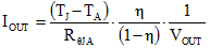
As with any power conversion device, the LMZ20501 will dissipate internal power while operating. The effect of this power dissipation is to raise the internal temperature of the converter above ambient. The internal die temperature is a function of the ambient temperature, the power loss, and the effective thermal resistance RθJA of the device and PCB combination. The maximum internal die temperature for the LMZ20501 is 125°C, thus establishing a limit on the maximum device power dissipation and, therefore, load current at high ambient temperatures. Equation 3 shows the relationships between the important parameters.

Equation 3. GUID-F02D7AC9-4A66-49D1-BC57-5DA8EA16651A-low.gif

It is easy to see that larger ambient temperatures and larger values of RθJA will reduce the maximum available output current. As stated in the Semiconductor and IC Package Thermal Metrics Application Report, the values given in the Thermal Information table are not valid for design purposes and must not be used to estimate the thermal performance of the application. The values reported in that table were measured under a specific set of conditions that never obtain in an actual application. The effective RθJA is a critical parameter and depends on many factors such as the following:

  • Power dissipation
  • Air temperature
  • PCB area
  • Copper heatsink area
  • Air flow
  • Adjacent component placement
The resources found in Table 11-1 can be used as a guide to estimate the RθJA for a given application environment. A typical example of RθJA versus copper board area is shown in Figure 8-3. The copper area in this graph is that for each layer; the inner layers are 1 oz (35µm). An RθJA of 44°C/W is the approximate value for the LMZ20501 evaluation board. The efficiency found in Equation 3, η, should be taken at the elevated ambient temperature. For the LMZ20501, the efficiency is approximately two to three percent lower at high temperatures. Therefore, a slightly lower value than the typical efficiency can be used in the calculation. In this way, Equation 3 can be used to estimate the maximum output current for a given ambient, or to estimate the maximum ambient for a given load current.

A typical curve of maximum load current versus ambient temperature is shown in Figure 8-4. This graph assumes a RθJA of 44°C/W and an input voltage of 5 V.

GUID-524DD6EE-2492-4310-84EF-33DBE8CF1B56-low.gifFigure 8-3 RθJA Versus Copper Board Area
GUID-79527077-3E69-44C8-927C-65FEC2F88A3E-low.pngFigure 8-4 Maximum Output Current Versus Ambient Temperature, RθJA = 44°C/W, VIN = 5 V