ZHCSDN1E August 2012 – September 2021 LMZ20501
PRODUCTION DATA
- 1 特性
- 2 应用
- 3 说明
- 4 Revision History
- 5 Pin Configuration and Functions
- 6 Specifications
- 7 Detailed Description
- 8 Application and Implementation
- 9 Power Supply Recommendations
- 10Layout
- 11Device and Documentation Support
- 12Mechanical, Packaging, and Orderable Information
9 Power Supply Recommendations
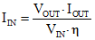
The characteristics of the input supply must be compatible with the Absolute Maximum Ratings and Recommended Operating Conditions found in this data sheet. In addition, the input supply must be capable of delivering the required input current to the loaded regulator. The average input current can be estimated with Equation 4
If the regulator is connected to the input supply through long wires or PCB traces, special care is required to achieve good performance. The parasitic inductance and resistance of the input cables can have an adverse effect on the operation of the regulator. The parasitic inductance, in combination with the low ESR ceramic input capacitors, can form an under-damped resonant circuit. This circuit can cause overvoltage transients at the VIN pin, each time the input supply is cycled on and off. The parasitic resistance will cause the voltage at the VIN pin to dip when the load on the regulator is switched on, or exhibits a transient. If the regulator is operating close to the minimum input voltage, this dip can cause the device to shutdown, reset, or both. The best way to solve these kinds of issues is to reduce the distance from the input supply to the regulator, use an aluminum or tantalum input capacitor in parallel with the ceramics, or both. The moderate ESR of these types of capacitors will help to damp the input resonant circuit and reduce any voltage overshoots. A value in the range of 20 µF to 100 µF is usually sufficient to provide input damping and help to hold the input voltage steady during large load transients.
Sometimes, for other system considerations, an input filter is used in front of the regulator module. This can lead to instability, as well as some of the effects mentioned above, unless it is designed carefully. The following user guide provides helpful suggestions when designing an input filter for any switching regulator: AN-2162 Simple Success With Conducted EMI From DC-DC Converters Application Report.
In some cases, a Transient Voltage Suppressor (TVS) is used on the input of regulators. One class of this device has a "snap-back" V-I characteristic (thyristor type). The use of a device with this type of characteristic is not recommend. When the TVS "fires", the clamping voltage drops to a very low value. If this holding voltage is less than the output voltage of the regulator, the output capacitors will be discharged through the regulator back to the input. This uncontrolled current flow could damage the regulator.