ZHCSDN1E August 2012 – September 2021 LMZ20501
PRODUCTION DATA
- 1 特性
- 2 应用
- 3 说明
- 4 Revision History
- 5 Pin Configuration and Functions
- 6 Specifications
- 7 Detailed Description
- 8 Application and Implementation
- 9 Power Supply Recommendations
- 10Layout
- 11Device and Documentation Support
- 12Mechanical, Packaging, and Orderable Information
10.2.1 Soldering Information
Proper operation of the LMZ20501 requires that it be correctly soldered to the PCB. This is especially true regarding the EP. This pad acts as a quiet ground reference for the device and a heatsink connection. Use the following recommendations when utilizing machine placement of the device:
- Dimension of area for pickup: 2 mm × 2.5 mm
- Use a nozzle size of less than 1.3 mm in diameter, so that the head does not touch the outer area of the package.
- Use a soft tip pick-and-place head.
- Add 0.05 mm to the component thickness so that the device will be released 0.05 mm into the solder paste without putting pressure or splashing the solder paste.
- Slow the pick arm when picking the part from the tape and reel carrier and when depositing the device on the board.
- If the machine releases the component by force, use the minimum force and no more than 3 N.
- For PCBs with surface mount components on both sides, it is suggested to put the LMZ20501 on the top side. In case the application requires bottom side placement, a re-flow fixture can be required to protect the module during the second reflow.
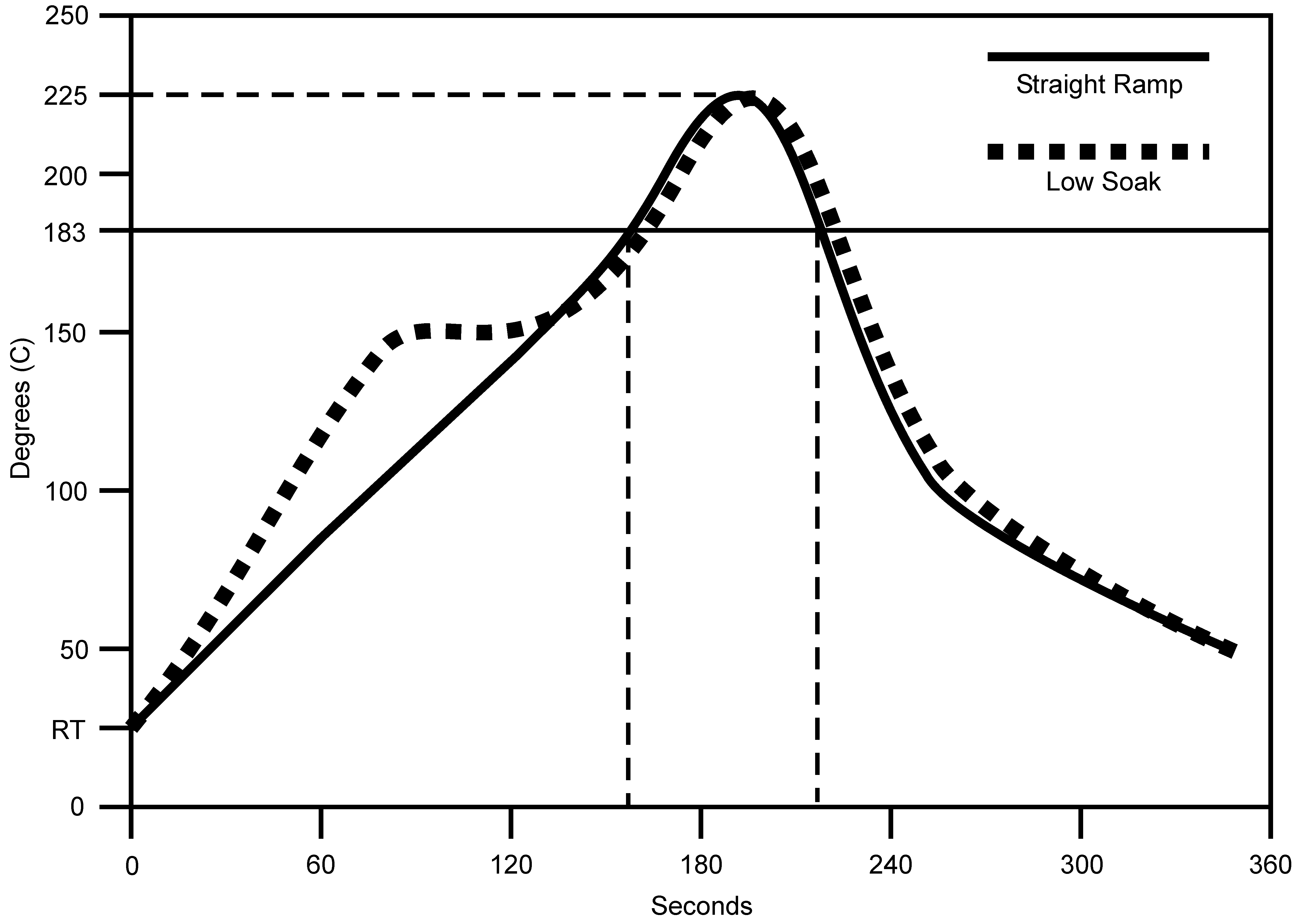
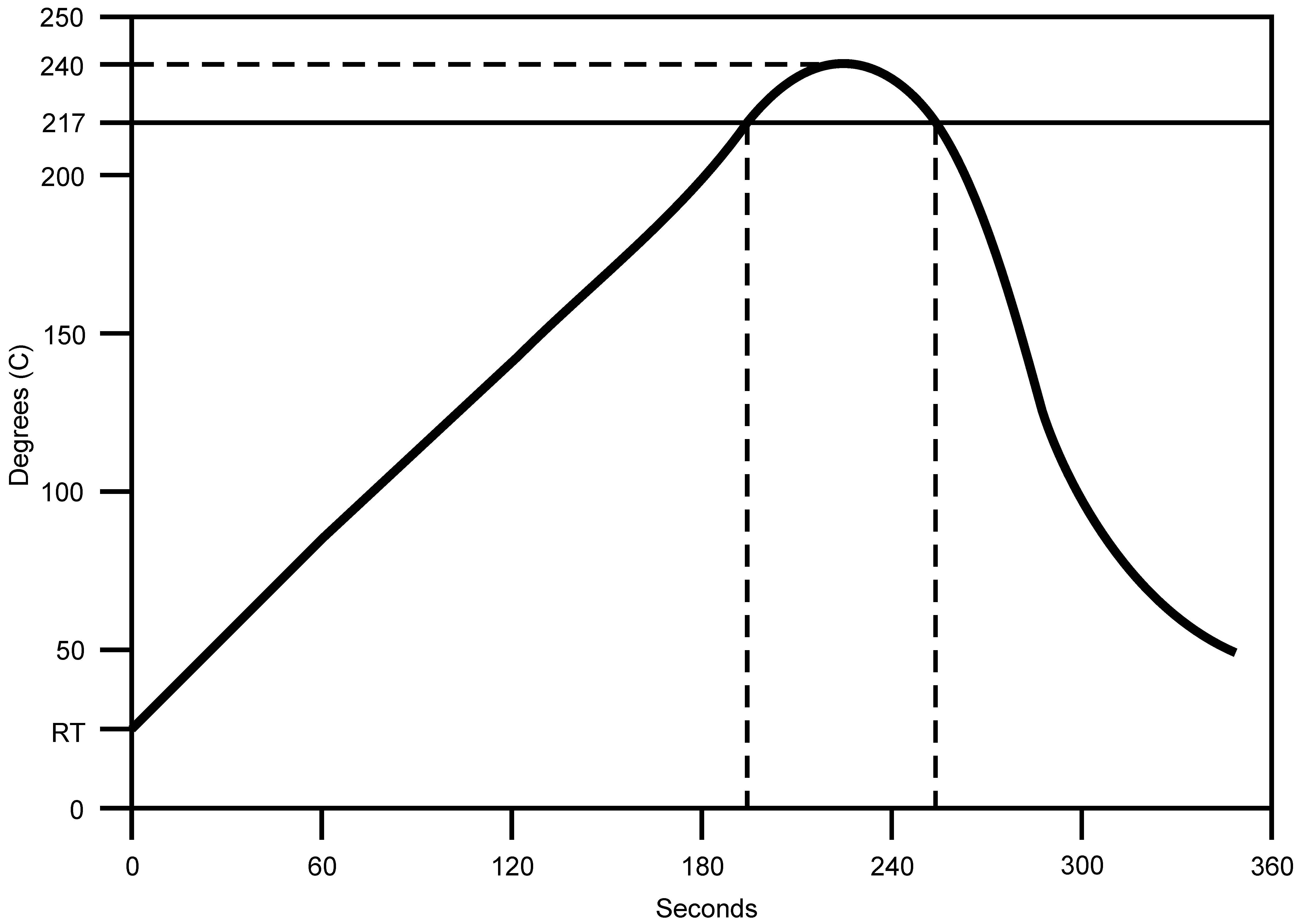
In addition, please follow the important guidelines found in the AN-1187 Leadless Leadframe Package (LLP) Application Report. The curves in Figure 10-3 and Figure 10-4 show typical soldering temperature profiles.
 Figure 10-3 Typical Re-flow Profile Eutectic (63sn/37pb) Solder Paste
 Figure 10-4 Typical Re-flow Profile Lead-Free (Sca305 Or Sac405) Solder Paste