ZHCSDN1E August   2012  – September 2021 LMZ20501

PRODUCTION DATA  

  1. 特性
  2. 应用
  3. 说明
  4. Revision History
  5. Pin Configuration and Functions
  6. Specifications
    1. 6.1 Absolute Maximum Ratings
    2. 6.2 ESD Ratings
    3. 6.3 Recommended Operating Conditions
    4. 6.4 Thermal Information
    5. 6.5 Electrical Characteristics
    6. 6.6 System Characteristics
    7. 6.7 Typical Characteristics
  7. Detailed Description
    1. 7.1 Overview
    2. 7.2 Functional Block Diagram
    3. 7.3 Feature Description
      1. 7.3.1 Nano Scale Package
      2. 7.3.2 Internal Synchronous Rectifier
      3. 7.3.3 Current Limit Protection
      4. 7.3.4 Start-Up
      5. 7.3.5 Dropout Behavior
      6. 7.3.6 Power Good Flag Function
      7. 7.3.7 Thermal Shutdown
    4. 7.4 Device Functional Modes
      1. 7.4.1 PWM Operation
      2. 7.4.2 PFM Operation
  8. Application and Implementation
    1. 8.1 Application Information
    2. 8.2 Typical Application
      1. 8.2.1 Detailed Design Procedure
        1. 8.2.1.1 Custom Design With WEBENCH® Tools
        2. 8.2.1.2 Setting The Output Voltage
        3. 8.2.1.3 Output and Feedforward Capacitors
        4. 8.2.1.4 Input Capacitors
        5. 8.2.1.5 Maximum Ambient Temperature
        6. 8.2.1.6 Options
      2. 8.2.2 Application Curves
    3. 8.3 Do's and Don'ts
  9. Power Supply Recommendations
  10. 10Layout
    1. 10.1 Layout Guidelines
    2. 10.2 Layout Example
      1. 10.2.1 Soldering Information
  11. 11Device and Documentation Support
    1. 11.1 Device Support
      1. 11.1.1 第三方产品免责声明
      2. 11.1.2 Development Support
        1. 11.1.2.1 Custom Design With WEBENCH® Tools
    2. 11.2 Documentation Support
      1. 11.2.1 Related Documentation
    3. 11.3 接收文档更新通知
    4. 11.4 支持资源
    5. 11.5 Trademarks
    6. 11.6 Electrostatic Discharge Caution
    7. 11.7 术语表
  12. 12Mechanical, Packaging, and Orderable Information
    1. 12.1 Tape and Reel Information

封装选项

请参考 PDF 数据表获取器件具体的封装图。

机械数据 (封装 | 引脚)
  • SIL|8
散热焊盘机械数据 (封装 | 引脚)
订购信息

Power Good Flag Function

The operation of the power good flag function is described in the diagram shown in Figure 7-7.
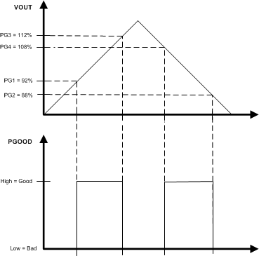
GUID-811360F4-EBED-4E04-8E2A-358E994B0EC5-low.gif Figure 7-7 Typical Power Good-Flag Operation

This output consists of an open-drain NMOS with an Rdson of approximately 70 Ω. When used, the power-good flag should be connected to a logic supply through a pullup resistor. It can also be pulled up to either VIN or VOUT through an appropriate resistor, as desired. If this function is not needed, the PG output should be left floating. The current through this flag pin should be limited to less than 4 mA. A pullup resistor of greater than or equal to 1.5 kΩ will satisfy this requirement. When the EN input is pulled low, the PG flag output will also be forced low, assuming a valid input voltage is present at the VIN pin.