ZHCSF93E December 2015 – August 2020 LMR23630
PRODUCTION DATA
- 1 特性
- 2 应用
- 3 说明
- 4 Revision History
- 5 Device Comparison Table
- 6 Pin Configuration and Functions
- 7 Specifications
-
8 Detailed Description
- 8.1 Overview
- 8.2 Functional Block Diagram
- 8.3
Feature Description
- 8.3.1 Fixed Frequency Peak Current Mode Control
- 8.3.2 Adjustable Frequency
- 8.3.3 Adjustable Output Voltage
- 8.3.4 Enable/Sync
- 8.3.5 VCC, UVLO
- 8.3.6 Minimum ON-time, Minimum OFF-time and Frequency Foldback at Dropout Conditions
- 8.3.7 Power Good (PGOOD)
- 8.3.8 Internal Compensation and CFF
- 8.3.9 Bootstrap Voltage (BOOT)
- 8.3.10 Overcurrent and Short-Circuit Protection
- 8.3.11 Thermal Shutdown
- 8.4 Device Functional Modes
-
9 Application and Implementation
- 9.1 Application Information
- 9.2
Typical Applications
- 9.2.1 Design Requirements
- 9.2.2
Detailed Design Procedure
- 9.2.2.1 Custom Design With WEBENCH® Tools
- 9.2.2.2 Output Voltage Setpoint
- 9.2.2.3 Switching Frequency
- 9.2.2.4 Inductor Selection
- 9.2.2.5 Output Capacitor Selection
- 9.2.2.6 Feed-Forward Capacitor
- 9.2.2.7 Input Capacitor Selection
- 9.2.2.8 Bootstrap Capacitor Selection
- 9.2.2.9 VCC Capacitor Selection
- 9.2.2.10 Undervoltage Lockout Setpoint
- 9.2.3 Application Curves
- 10Power Supply Recommendations
- 11Layout
- 12Device and Documentation Support
- 13Mechanical, Packaging, and Orderable Information
封装选项
请参考 PDF 数据表获取器件具体的封装图。
机械数据 (封装 | 引脚)
- DRR|12
- DDA|8
散热焊盘机械数据 (封装 | 引脚)
订购信息
8.3.10 Overcurrent and Short-Circuit Protection
The LMR23630 is protected from over-current conditions by cycle-by-cycle current limit on both the peak and valley of the inductor current. Hiccup mode will be activated if a fault condition persists to prevent over-heating.
High-side MOSFET overcurrent protection is implemented by the nature of the peak-current-mode control. The HS switch current is sensed when the HS is turned on after a set blanking time. The HS switch current is compared to the output of the error amplifier (EA) minus slope compensation every switching cycle. See the Section 8.2 for more details. The peak current of HS switch is limited by a clamped maximum peak current threshold IHS_LIMIT which is constant. Thus, the peak current limit of the high-side switch is not affected by the slope compensation and remains constant over the full duty cycle range.
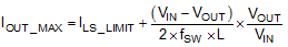
The current going through LS MOSFET is also sensed and monitored. When the LS switch turns on, the inductor current begins to ramp down. The LS switch is not turned OFF at the end of a switching cycle if its current is above the LS current limit ILS_LIMIT. The LS switch is kept ON so that inductor current keeps ramping down, until the inductor current ramps below the LS current limit ILS_LIMIT. Then the LS switch is turned OFF, and the HS switch is turned on after a dead time. This is somewhat different than the more typical peak current limit and results in Equation 10 for the maximum load current.
If the current of the LS switch is higher than the LS current limit for 64 consecutive cycles, hiccup current protection mode is activated. In hiccup mode, the regulator is shut down and kept off for 5 ms typically before the LMR23630 tries to start again. If overcurrent or short-circuit fault condition still exist, hiccup will repeat until the fault condition is removed. Hiccup mode reduces power dissipation under severe overcurrent conditions, prevents over-heating and potential damage to the device.
For FPWM version, the inductor current is allowed to go negative. If this current exceed IL_NEG, the LS switch is turned off until the next clock cycle. This is used to protect the LS switch from excessive negative current.