ZHCSIN4B August 2018 – June 2021 LM5146-Q1
PRODUCTION DATA
- 1 特性
- 2 应用
- 3 说明
- 4 Revision History
- 5 说明(续)
- 6 Pin Configuration and Functions
- 7 Specifications
-
8 Detailed Description
- 8.1 Overview
- 8.2 Functional Block Diagram
- 8.3
Feature Description
- 8.3.1 Input Range (VIN)
- 8.3.2 Output Voltage Setpoint and Accuracy (FB)
- 8.3.3 High-Voltage Bias Supply Regulator (VCC)
- 8.3.4 Precision Enable (EN/UVLO)
- 8.3.5 Power Good Monitor (PGOOD)
- 8.3.6 Switching Frequency (RT, SYNCIN)
- 8.3.7 Configurable Soft Start (SS/TRK)
- 8.3.8 Voltage-Mode Control (COMP)
- 8.3.9 Gate Drivers (LO, HO)
- 8.3.10 Current Sensing and Overcurrent Protection (ILIM)
- 8.3.11 OCP Duty Cycle Limiter
- 8.4 Device Functional Modes
- 9 Application and Implementation
- 10Power Supply Recommendations
- 11Layout
- 12Device and Documentation Support
- 13Mechanical, Packaging, and Orderable Information
封装选项
请参考 PDF 数据表获取器件具体的封装图。
机械数据 (封装 | 引脚)
- RGY|20
散热焊盘机械数据 (封装 | 引脚)
- RGY|20
订购信息
9.1.3 Control Loop Compensation
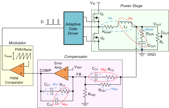
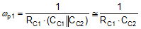
The poles and zeros inherent to the power stage and compensator are respectively illustrated by red and blue dashed rings in the schematic embedded in Table 9-2. The compensation network typically employed with voltage-mode control is a Type-III circuit with three poles and two zeros. One compensator pole is located at the origin to realize high DC gain. The normal compensation strategy uses two compensator zeros to counteract the LC double pole, one compensator pole located to nullify the output capacitor ESR zero, with the remaining compensator pole located at one-half switching frequency to attenuate high frequency noise. The resistor divider network to FB determines the desired output voltage. Note that the lower feedback resistor, RFB2, has no impact on the control loop from an AC standpoint because the FB node is the input to an error amplifier and is effectively at AC ground. Hence, the control loop is designed irrespective of output voltage level. The proviso here is the necessary output capacitance derating with bias voltage and temperature.
 |
|||
|---|---|---|---|
| POWER STAGE POLES | POWER STAGE ZEROS | COMPENSATOR POLES | COMPENSATOR ZEROS |
 (1)(2) (1)(2) |
 |
 |
 |
 |
 |
 |
|
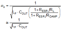
The small-signal open-loop response of a buck regulator is the product of modulator, power train and compensator transfer functions. The power stage transfer function can be represented as a complex pole pair associated with the output LC filter and a zero related to the ESR of the output capacitor. The DC (and low frequency) gain of the modulator and power stage is VIN/VRAMP. The gain from COMP to the average voltage at the input of the LC filter is held essentially constant by the PWM line feedforward feature of the LM5146-Q1 (15 V/V or 23.5 dB).
Complete expressions for small-signal frequency analysis are presented in Table 9-3. The transfer functions are denoted in normalized form. While the loop gain is of primary importance, a regulator is not specified directly by its loop gain but by its performance related characteristics, namely closed-loop output impedance and audio susceptibility.
| TRANSFER FUNCTION | EXPRESSION |
|---|---|
| Open-loop transfer function | 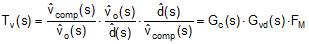 |
| Duty-cycle-to-output transfer function | 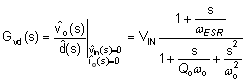 |
| Compensator transfer function(1) | 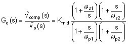 |
| Modulator transfer function | 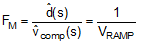 |
Figure 9-2 shows the open-loop response gain and phase. The poles and zeros of the system are marked with x and o symbols, respectively, and a + symbol indicates the crossover frequency. When plotted on a log (dB) scale, the open-loop gain is effectively the sum of the individual gain components from the modulator, power stage, and compensator (see Figure 9-3). The open-loop response of the system is measured experimentally by breaking the loop, injecting a variable-frequency oscillator signal, and recording the ensuing frequency response using a network analyzer setup.
 Figure 9-2 Typical Buck Regulator Loop Gain and Phase With Voltage-Mode Control
If the pole located at ωp1 cancels the zero located at ωESR and the pole at ωp2 is located well above crossover, the expression for the loop gain, Tv(s) in Table 9-3, can be manipulated to yield the simplified expression given in Equation 14.
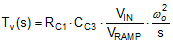
Essentially, a multi-order system is reduced to a single-order approximation by judicious choice of compensator components. A simple solution for the crossover frequency (denoted as fc in Figure 9-2) with Type-III voltage-mode compensation is derived as shown in Equation 15 and Equation 16.
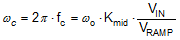
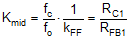
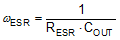
 Figure 9-3 Buck Regulator Constituent Gain Components
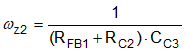
The loop crossover frequency is usually selected between one-tenth to one-fifth of switching frequency. Inserting an appropriate crossover frequency into Equation 16 gives a target for the mid-band gain of the compensator, Kmid. Given an initial value for RFB1, RFB2 is then selected based on the desired output voltage. Values for RC1, RC2, CC1, CC2, and CC3 are calculated from the design expressions listed in Table 9-4, with the premise that the compensator poles and zeros are set as follows: ωz1 = 0.5·ωo, ωz2 = ωo, ωp1 = ωESD, and ωp2 = ωSW / 2.
| RESISTORS | CAPACITORS |
|---|---|
 |
 |
 |
 |
 |
 |
Referring to the bode plot in Figure 9-2, the phase margin, indicated as φM, is the difference between the loop phase and –180° at crossover. A target of 50° to 70° for this parameter is considered ideal. Additional phase boost is dialed in by locating the compensator zeros at a frequency lower than the LC double pole. This helps mitigate the phase dip associated with the LC filter, particularly at light loads when the Q-factor is higher and the phase dip becomes especially prominent. The ramification of low phase in the frequency domain is an under-damped transient response in the time domain.
The power supply designer now has all the necessary expressions to optimally position the loop crossover frequency while maintaining adequate phase margin over the required line, load and temperature operating ranges. The LM5146-Q1 Quickstart Calculator is available to expedite these calculations and to adjust the bode plot as needed.