ZHCSIN4B August 2018 – June 2021 LM5146-Q1
PRODUCTION DATA
- 1 特性
- 2 应用
- 3 说明
- 4 Revision History
- 5 说明(续)
- 6 Pin Configuration and Functions
- 7 Specifications
-
8 Detailed Description
- 8.1 Overview
- 8.2 Functional Block Diagram
- 8.3
Feature Description
- 8.3.1 Input Range (VIN)
- 8.3.2 Output Voltage Setpoint and Accuracy (FB)
- 8.3.3 High-Voltage Bias Supply Regulator (VCC)
- 8.3.4 Precision Enable (EN/UVLO)
- 8.3.5 Power Good Monitor (PGOOD)
- 8.3.6 Switching Frequency (RT, SYNCIN)
- 8.3.7 Configurable Soft Start (SS/TRK)
- 8.3.8 Voltage-Mode Control (COMP)
- 8.3.9 Gate Drivers (LO, HO)
- 8.3.10 Current Sensing and Overcurrent Protection (ILIM)
- 8.3.11 OCP Duty Cycle Limiter
- 8.4 Device Functional Modes
- 9 Application and Implementation
- 10Power Supply Recommendations
- 11Layout
- 12Device and Documentation Support
- 13Mechanical, Packaging, and Orderable Information
封装选项
请参考 PDF 数据表获取器件具体的封装图。
机械数据 (封装 | 引脚)
- RGY|20
散热焊盘机械数据 (封装 | 引脚)
- RGY|20
订购信息
8.3.4 Precision Enable (EN/UVLO)
The EN/UVLO input supports adjustable input undervoltage lockout (UVLO) with hysteresis programmed by the resistor values for application specific power-up and power-down requirements. EN/UVLO connects to a comparator-based input referenced to a 1.2-V bandgap voltage. An external logic signal can be used to drive the EN/UVLO input to toggle the output ON and OFF and for system sequencing or protection. The simplest way to enable the operation of the LM5146-Q1 is to connect EN/UVLO directly to VIN. This allows self start-up of the LM5146-Q1 when VCC is within its valid operating range. However, many applications benefit from using a resistor divider RUV1 and RUV2 as shown in Figure 8-3 to establish a precision UVLO level.
Use Equation 1 and Equation 2 to calculate the UVLO resistors given the required input turn-on and turn-off voltages.
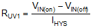
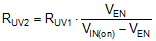
 Figure 8-3 Programmable Input Voltage
UVLO Turn-on and Turn-off
Figure 8-3 Programmable Input Voltage
UVLO Turn-on and Turn-offThe LM5146-Q1 enters a low IQ shutdown mode when EN/UVLO is pulled below approximately 0.4 V. The internal LDO regulator powers off and the internal bias supply rail collapses, shutting down the bias currents of the LM5146-Q1. The LM5146-Q1 operates in standby mode when the EN/UVLO voltage is between the hard shutdown and precision enable (standby) thresholds.