ZHCSIN4B August   2018  – June 2021 LM5146-Q1

PRODUCTION DATA  

  1. 特性
  2. 应用
  3. 说明
  4. Revision History
  5. 说明(续)
  6. Pin Configuration and Functions
    1. 6.1 Wettable Flanks
  7. Specifications
    1. 7.1 Absolute Maximum Ratings
    2. 7.2 ESD Ratings 
    3. 7.3 Recommended Operating Conditions
    4. 7.4 Thermal Information
    5. 7.5 Electrical Characteristics
    6. 7.6 Switching Characteristics
    7. 7.7 Typical Characteristics
  8. Detailed Description
    1. 8.1 Overview
    2. 8.2 Functional Block Diagram
    3. 8.3 Feature Description
      1. 8.3.1  Input Range (VIN)
      2. 8.3.2  Output Voltage Setpoint and Accuracy (FB)
      3. 8.3.3  High-Voltage Bias Supply Regulator (VCC)
      4. 8.3.4  Precision Enable (EN/UVLO)
      5. 8.3.5  Power Good Monitor (PGOOD)
      6. 8.3.6  Switching Frequency (RT, SYNCIN)
        1. 8.3.6.1 Frequency Adjust
        2. 8.3.6.2 Clock Synchronization
      7. 8.3.7  Configurable Soft Start (SS/TRK)
        1. 8.3.7.1 Tracking
      8. 8.3.8  Voltage-Mode Control (COMP)
      9. 8.3.9  Gate Drivers (LO, HO)
      10. 8.3.10 Current Sensing and Overcurrent Protection (ILIM)
      11. 8.3.11 OCP Duty Cycle Limiter
    4. 8.4 Device Functional Modes
      1. 8.4.1 Shutdown Mode
      2. 8.4.2 Standby Mode
      3. 8.4.3 Active Mode
      4. 8.4.4 Diode Emulation Mode
      5. 8.4.5 Thermal Shutdown
  9. Application and Implementation
    1. 9.1 Application Information
      1. 9.1.1 Design and Implementation
      2. 9.1.2 Power Train Components
        1. 9.1.2.1 Inductor
        2. 9.1.2.2 Output Capacitors
        3. 9.1.2.3 Input Capacitors
        4. 9.1.2.4 Power MOSFETs
      3. 9.1.3 Control Loop Compensation
      4. 9.1.4 EMI Filter Design
    2. 9.2 Typical Applications
      1. 9.2.1 Design 1 – 12-A High-Efficiency Synchronous Buck DC/DC Regulator for Automotive Applications
        1. 9.2.1.1 Design Requirements
        2. 9.2.1.2 Detailed Design Procedure
        3. 9.2.1.3 Custom Design With WEBENCH® Tools
        4. 9.2.1.4 Custom Design With Excel Quickstart Tool
        5. 9.2.1.5 Application Curves
      2. 9.2.2 Design 2 – High Density, 12-V, 8-A Rail From 48-V Automotive Battery Power
        1. 9.2.2.1 Design Requirements
        2. 9.2.2.2 Detailed Design Procedure
        3. 9.2.2.3 Application Curves
  10. 10Power Supply Recommendations
  11. 11Layout
    1. 11.1 Layout Guidelines
      1. 11.1.1 Power Stage Layout
      2. 11.1.2 Gate Drive Layout
      3. 11.1.3 PWM Controller Layout
      4. 11.1.4 Thermal Design and Layout
      5. 11.1.5 Ground Plane Design
    2. 11.2 Layout Example
  12. 12Device and Documentation Support
    1. 12.1 Device Support
      1. 12.1.1 第三方产品免责声明
      2. 12.1.2 Development Support
        1. 12.1.2.1 Custom Design With WEBENCH® Tools
    2. 12.2 Documentation Support
      1. 12.2.1 Related Documentation
        1. 12.2.1.1 PCB Layout Resources
        2. 12.2.1.2 Thermal Design Resources
    3. 12.3 接收文档更新通知
    4. 12.4 支持资源
    5. 12.5 Trademarks
    6. 12.6 Electrostatic Discharge Caution
    7. 12.7 Glossary
  13. 13Mechanical, Packaging, and Orderable Information

封装选项

请参考 PDF 数据表获取器件具体的封装图。

机械数据 (封装 | 引脚)
  • RGY|20
散热焊盘机械数据 (封装 | 引脚)
订购信息

Layout Guidelines

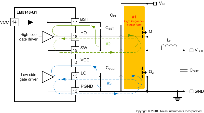
Proper PCB design and layout is important in a high-current, fast-switching circuits (with high current and voltage slew rates) to assure appropriate device operation and design robustness. As expected, certain issues must be considered before designing a PCB layout using the LM5146-Q1. The high-frequency power loop of the buck converter power stage is denoted by #1 in the shaded area of Figure 11-1. The topological architecture of a buck converter means that particularly high di/dt current flows in the components of loop 1, and it becomes mandatory to reduce the parasitic inductance of this loop by minimizing its effective loop area. Also important is the gate drive loops of the low-side and high-side MOSFETs, denoted by 2 and 3, respectively, in Figure 11-1.
GUID-2C1E28C4-AF33-4524-9D52-E14CD0982AC2-low.gifFigure 11-1 DC/DC Regulator Ground System With Power Stage and Gate Drive Circuit Switching Loops