SNVS424D January 2006 – December 2014 LM5106
PRODUCTION DATA.
6 Specifications
6.1 Absolute Maximum Ratings(1)(1)
| MIN | MAX | UNIT | |
|---|---|---|---|
| VDD to VSS | –0.3 | 18 | V |
| HB to HS | –0.3 | 18 | V |
| IN and EN to VSS | –0.3 | VDD + 0.3 | V |
| LO to VSS | –0.3 | VDD + 0.3 | V |
| HO to VSS | HS – 0.3 | HB + 0.3 | V |
| HS to VSS(5) | 100 | V | |
| HB to VSS | 118 | V | |
| RDT to VSS | –0.3 | 5 | V |
| Junction Temperature | 150 | °C | |
| Storage temperature range, Tstg | –55 | 150 | °C |
(1) If Military/Aerospace specified devices are required, please contact the Texas Instruments Sales Office/Distributors for availability and specifications.
6.2 ESD Ratings
| VALUE | UNIT | |||
|---|---|---|---|---|
| V(ESD) | Electrostatic discharge | Human body model (HBM), per ANSI/ESDA/JEDEC JS-001(1) | ±1500 | V |
(1) JEDEC document JEP155 states that 500-V HBM allows safe manufacturing with a standard ESD control process.
6.3 Recommended Operating Conditions
| MIN | MAX | UNIT | |
|---|---|---|---|
| VDD | 8 | 14 | V |
| HS(5) | –1 | 100 | V |
| HB | HS + 8 | HS + 14 | V |
| HS Slew Rate | < 50 | V/ns | |
| Junction Temperature | –40 | 125 | °C |
6.4 Thermal Information
| THERMAL METRIC(1) | LM5102 | UNIT | ||
|---|---|---|---|---|
| DGS | DPR(2) | |||
| 10 PINS | 10 PINS | |||
| RθJA | Junction-to-ambient thermal resistance | 165.3 | 37.9 | °C/W |
| RθJC(top) | Junction-to-case (top) thermal resistance | 58.9 | 38.1 | |
| RθJB | Junction-to-board thermal resistance | 54.4 | 14.9 | |
| ψJT | Junction-to-top characterization parameter | 6.2 | 0.4 | |
| ψJB | Junction-to-board characterization parameter | 83.6 | 15.2 | |
| RθJC(bot) | Junction-to-case (bottom) thermal resistance | N/A | 4.4 | |
(1) For more information about traditional and new thermal metrics, see the IC Package Thermal Metrics application report (SPRA953).
(2) Four-layer board with Cu finished thickness 1.5 oz, 1 oz, 1 oz, 1.5 oz. Maximum die size used. 5x body length of Cu trace on PCB top. 50-mm × 50-mm ground and power planes embedded in PCB. See Application Note AN-1187 Leadless Leadframe Package (LLP) (SNOA401).
6.5 Electrical Characteristics
MIN and MAX limits apply over the full operating junction temperature range. Unless otherwise specified, TJ = +25°C, VDD = HB = 12 V, VSS = HS = 0 V, EN = 5 V. No load on LO or HO. RDT= 100kΩ(3).| SYMBOL | PARAMETER | TEST CONDITIONS | MIN | TYP | MAX | UNIT |
|---|---|---|---|---|---|---|
| SUPPLY CURRENTS | ||||||
| IDD | VDD Quiescent Current | IN = EN = 0 V | 0.34 | 0.6 | mA | |
| IDDO | VDD Operating Current | f = 500 kHz | 2.1 | 3.5 | mA | |
| IHB | Total HB Quiescent Current | IN = EN = 0 V | 0.06 | 0.2 | mA | |
| IHBO | Total HB Operating Current | f = 500 kHz | 1.5 | 3 | mA | |
| IHBS | HB to VSS Current, Quiescent | HS = HB = 100 V | 0.1 | 10 | µA | |
| IHBSO | HB to VSS Current, Operating | f = 500 kHz | 0.5 | mA | ||
| INPUT IN and EN | ||||||
| VIL | Low Level Input Voltage Threshold | 0.8 | 1.8 | V | ||
| VIH | High Level Input Voltage Threshold | 1.8 | 2.2 | V | ||
| Rpd | Input Pulldown Resistance Pin IN and EN | 100 | 200 | 500 | kΩ | |
| DEAD-TIME CONTROLS | ||||||
| VRDT | Nominal Voltage at RDT | 2.7 | 3 | 3.3 | V | |
| IRDT | RDT Pin Current Limit | RDT = 0 V | 0.75 | 1.5 | 2.25 | mA |
| UNDERVOLTAGE PROTECTION | ||||||
| VDDR | VDD Rising Threshold | 6.2 | 6.9 | 7.6 | V | |
| VDDH | VDD Threshold Hysteresis | 0.5 | V | |||
| VHBR | HB Rising Threshold | 5.9 | 6.6 | 7.3 | V | |
| VHBH | HB Threshold Hysteresis | 0.4 | V | |||
| LO GATE DRIVER | ||||||
| VOLL | Low-Level Output Voltage | ILO = 100 mA | 0.21 | 0.4 | V | |
| VOHL | High-Level Output Voltage | ILO = –100 mA, VOHL = VDD – VLO |
0.5 | 0.85 | V | |
| IOHL | Peak Pullup Current | LO = 0 V | 1.2 | A | ||
| IOLL | Peak Pulldown Current | LO = 12 V | 1.8 | A | ||
| HO GATE DRIVER | ||||||
| VOLH | Low-Level Output Voltage | IHO = 100 mA | 0.21 | 0.4 | V | |
| VOHH | High-Level Output Voltage | IHO = –100 mA, VOHH = HB – HO |
0.5 | 0.85 | V | |
| IOHH | Peak Pullup Current | HO = 0 V | 1.2 | A | ||
| IOLH | Peak Pulldown Current | HO = 12 V | 1.8 | A | ||
| THERMAL RESISTANCE | ||||||
| θJA | Junction to Ambient | See(2)(4) | 40 | °C/W | ||
6.6 Switching Characteristics
MIN and MAX limits apply over the full operating junction temperature range. Unless otherwise specified, TJ = +25°C, VDD = HB = 12 V, VSS = HS = 0 V, No Load on LO or HO(3).| SYMBOL | PARAMETER | TEST CONDITIONS | MIN | TYP | MAX | UNIT |
|---|---|---|---|---|---|---|
| tLPHL | Lower Turn-Off Propagation Delay | 32 | 56 | ns | ||
| tHPHL | Upper Turn-Off Propagation Delay | 32 | 56 | |||
| tLPLH | Lower Turn-On Propagation Delay | RDT = 100k | 400 | 520 | 640 | |
| tHPLH | Upper Turn-On Propagation Delay | RDT = 100k | 450 | 570 | 690 | |
| tLPLH | Lower Turn-On Propagation Delay | RDT = 10k | 85 | 115 | 160 | |
| tHPLH | Upper Turn-On Propagation Delay | RDT = 10k | 85 | 115 | 160 | |
| ten, tsd | Enable and Shutdown propagation delay | 36 | ||||
| DT1, DT2 | Dead-time LO OFF to HO ON & HO OFF to LO ON | RDT = 100k | 510 | |||
| RDT = 10k | 86 | |||||
| MDT | Dead-time matching | RDT = 100k | 50 | |||
| tR | Either Output Rise Time | CL = 1000pF | 15 | |||
| tF | Either Output Fall Time | CL = 1000pF | 10 |
(1) Absolute Maximum Ratings indicate limits beyond which damage to the component may occur. Recommended Operating Conditions are conditions under which operation of the device is ensured. Operating Ratings do not imply ensured performance limits. For ensured performance limits and associated test conditions, see the Electrical Characteristics.
(2) Four-layer board with Cu finished thickness 1.5/1.0/1.0/1.5 oz. Maximum die size used. 5x body length of Cu trace on PCB top. 50-mm × 50-mm ground and power planes embedded in PCB. See AN-1187 Leadless Leadframe Package (LLP), SNOA401.
(3) Min and Max limits are 100% production tested at 25°C. Limits over the operating temperature range are ensured through correlation using Statistical Quality Control (SQC) methods. Limits are used to calculate Average Outgoing Quality Level (AOQL).
(4) The θJA is not a constant for the package and depends on the printed circuit board design and the operating conditions.
(5) In the application the HS node is clamped by the body diode of the external lower N-MOSFET, therefore the HS voltage will generally not exceed –1 V. However in some applications, board resistance and inductance may result in the HS node exceeding this stated voltage transiently. If negative transients occur on HS, the HS voltage must never be more negative than VDD - 15 V. For example, if VDD = 10 V, the negative transients at HS must not exceed –5 V.
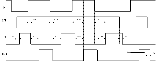 Figure 1. LM5106 Input - Output Waveforms
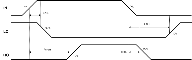 Figure 2. LM5106 Switching Time Definitions: tLPLH, tLPHL, tHPLH, tHPHL
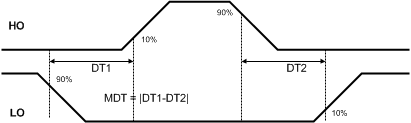 Figure 3. LM5106 Dead-time: DT
6.7 Typical Characteristics
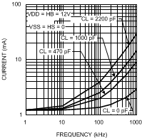 Figure 4. VDD Operating Current vs Frequency
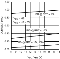 Figure 6. Quiescent Current vs Supply Voltage
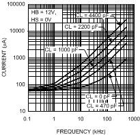 Figure 8. HB Operating Current vs Frequency
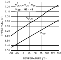 Figure 10. Undervoltage Rising Threshold vs Temperature
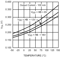 Figure 12. LO and HO - Low-Level Output Voltage vs Temperature
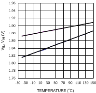 Figure 14. Input Threshold vs Temperature
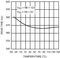 Figure 16. Dead-Time vs Temperature (RT = 100k)
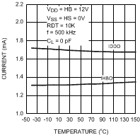 Figure 5. Operating Current vs Temperature
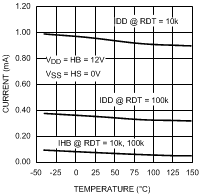 Figure 7. Quiescent Current vs Temperature
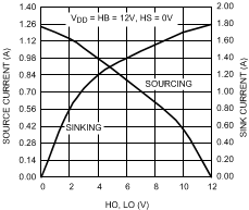 Figure 9. HO and LO Peak Output Current vs Output Voltage
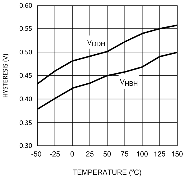 Figure 11. Undervoltage Hysteresis vs Temperature
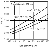 Figure 13. LO and HO - High-Level Output Voltage vs Temperature
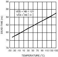 Figure 15. Dead-Time vs Temperature (RT = 10k)